
Non-volatile memory device and method of handling a datum read from a memory cell

A non-volatile memory technology, applied in static memory, read-only memory, digital memory information, etc., can solve the problem of high power consumption of memory devices

Active Publication Date: 2008-01-30
MICRON TECH INC
View PDF0 Cites 4 Cited by
  • Summary
  • Abstract
  • Description
  • Claims
  • Application Information

AI Technical Summary

Problems solved by technology

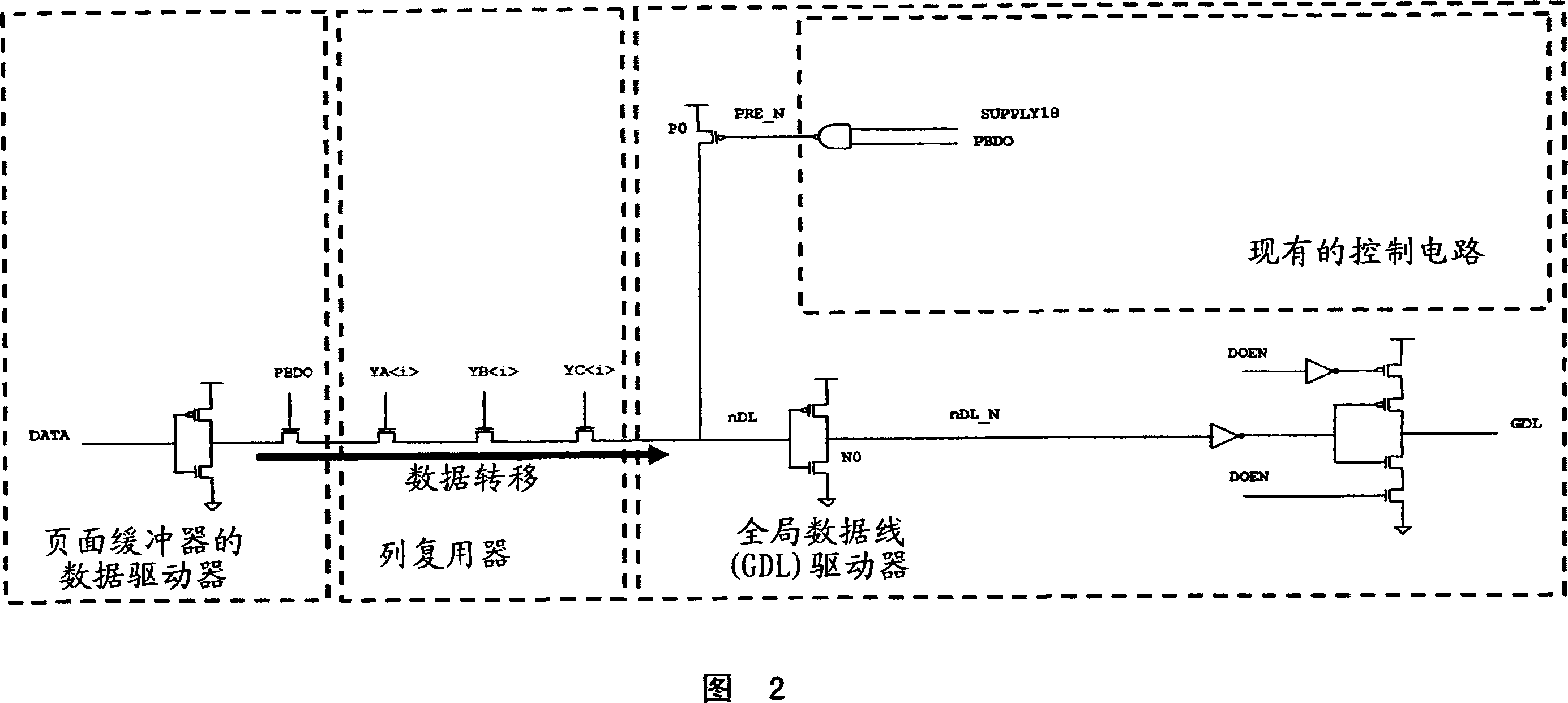
[0009] Unfortunately, it has been found that memory devices incorporating the circuit of Figure 2 consume more power than memory devices incorporating the circuit of Figure 1

Method used


Image

  • Non-volatile memory device and method of handling a datum read from a memory cell
  • Non-volatile memory device and method of handling a datum read from a memory cell
  • Non-volatile memory device and method of handling a datum read from a memory cell

Examples


Embodiment Construction

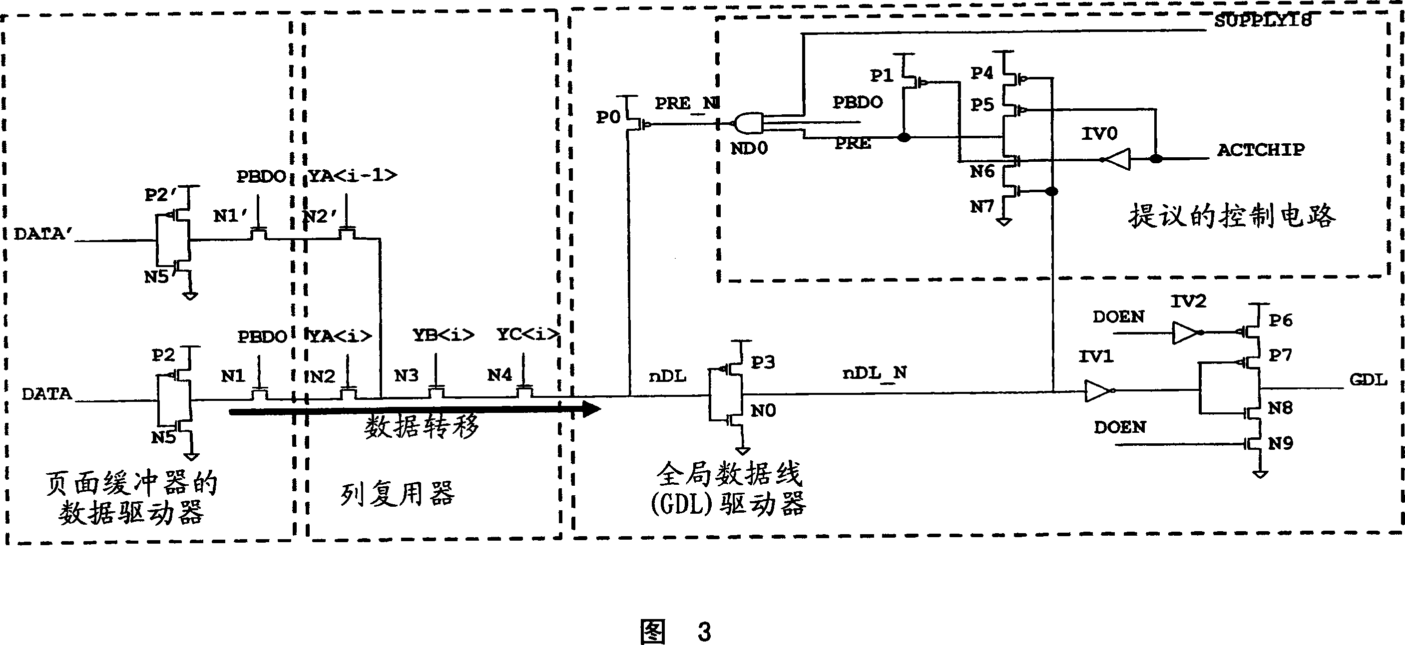
[0019] Fig. 3 shows a preferred embodiment of the global data line driver of the memory device of the present invention. Unlike the circuit shown in Figure 2, this novel global data line driver has a precharge control circuit that generates a control signal PRE_N such that the global The precharge transistor P0 is turned on only when the input line of the data line driver is precharged.

[0020] According to the method of the present invention, only when the external command SUPPLY18 is high level (that is, the memory device operates in a low voltage mode) at the same time, the enable signal PBDO is high level (that is, the page buffer is ready to output the read data) And when the internally generated auxiliary logic signal PRE is at a high level, the transistor P0 is turned on. When the standby signal ACTCHIP is high level (that is, the memory device is not in the standby state) or when the standby signal ACTCHIP is low level (that is, the memory device is in the standb...


PUM


Abstract

Memory devices that include a pre-charge transistor for connecting / disconnecting the input line of the global data line driver to a supply voltage line are more power consuming than the memory devices that do not include it because of a small though significant flow of current through the pre-charge transistor even in stand-by state. This problem is solved with a method implemented in a novel memory device, by turning on the pre-charge transistor only when, at the same time, the enabling signal of the page buffer is asserted, a low voltage functioning mode is selected and the memory device is not in a stand-by state, or the memory device is in a stand-by state but the datum read from the memory is high. The pre-charge transistor is securely turned off in all other cases.

Description

technical field [0001] The present invention relates to memory devices, and more particularly to memory devices including a global data line driver with an improved architecture to prevent errors in transferring read data to global data lines of the memory device. Background technique [0002] A non-volatile memory device organized and operating in a so-called page mode includes circuitry called a "page buffer" dedicated to storing data to be programmed at The data to be read from the addressed location of the cell array. The page buffer includes a data driver for each memory cell of a page for outputting read data. [0003] To understand the operation of the page buffer during a read operation, we refer to the classical scheme of Figure 1. Basically, during each read operation, when the enable signal PBDO is asserted, the data driver of the page buffer (PAGE BUFFER) transfers the data DATA read from each memory unit to the buffer output node. [0004] The output of the ...

Claims


Application Information

Patent Timeline
IPC IPC(8): G11C16/08
CPCG11C2207/2281G11C7/1069G11C7/1048G11C2207/002G11C7/1051
Inventor J·朴D·S·宋
Owner MICRON TECH INC
Learn More