Circuit arrangement and method of testing an application circuit provided in said circuit arrangement

A circuit device, circuit technology, applied in the direction of measuring device, measuring electricity, measuring electrical variables, etc., to achieve the effect of saving surface area

Inactive Publication Date: 2007-08-08
NXP BV
View PDF7 Cites 5 Cited by
  • Summary
  • Abstract
  • Description
  • Claims
  • Application Information

AI Technical Summary

Problems solved by technology

[0005] Here conventional implementations based on additional deterministic logic BIST hardware (so-called DLBIST hardware) result in practically large additional DLBIST hardware and larger integrated circuit devices

Method used


Image

  • Circuit arrangement and method of testing an application circuit provided in said circuit arrangement
  • Circuit arrangement and method of testing an application circuit provided in said circuit arrangement
  • Circuit arrangement and method of testing an application circuit provided in said circuit arrangement

Examples


Embodiment Construction

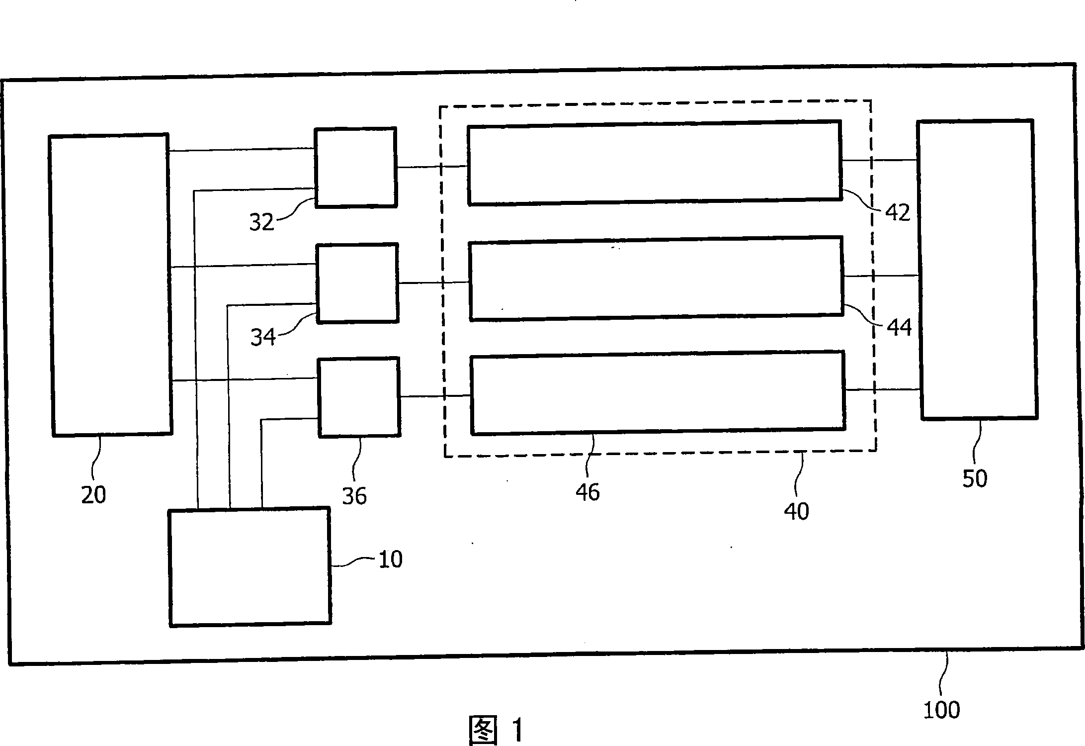
[0018] FIG. 1 is a block diagram of an integrated circuit device (IC) 100 including application circuitry 40 . The application circuit 40 is a circuit designed for the actual use purpose of the integrated circuit 100 .

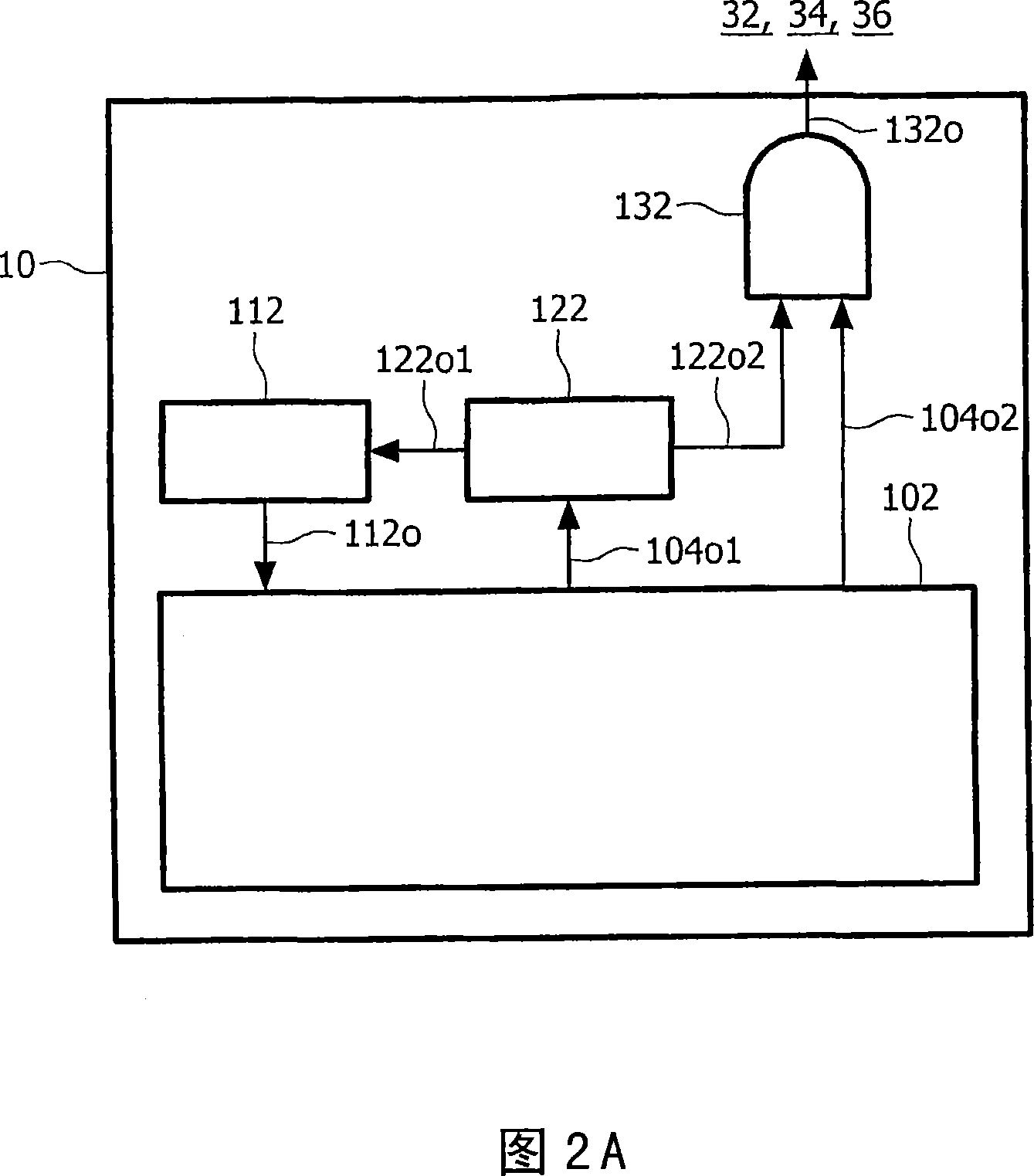
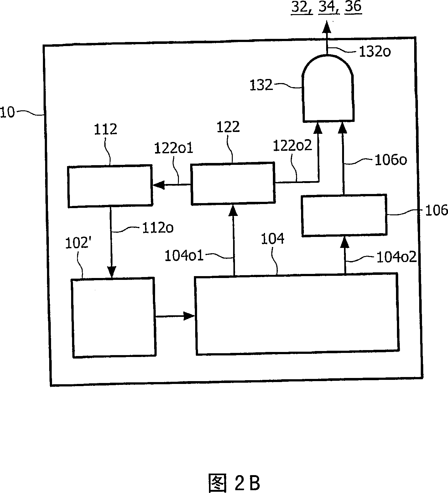
[0019] It is desirable to test application circuit 40 after fabrication of IC 100 in order to perfect operation. For this purpose, a self-test circuit is provided on the integrated circuit 100 , which self-test circuit comprises circuit elements 10 , 20 , 32 , 34 , 36 , 50 as shown in FIG. 1 .

[0020] The self-test circuit is designed in the integrated circuit 100 according to the invention in such a way that the relevant circuit elements 10, 20, 32, 34, 36, 50 are arranged completely outside the application circuit 40, so that the behavior of the application circuit 40 is normal. Unaffected by self-test circuitry during operation.

[0021] It is assumed that in the embodiment of FIG. 1 the application circuit 40 comprises two circuit chains (said scan chai...


PUM


Abstract

The object is to develop an integrated circuit arrangement (100) with at least one application circuit (40) to be tested. In addition, with at least one self-test circuit (10, 20, 32, 34, 36, 50) provided for testing the application circuit (40) and generating at least one pseudo-random test sample, wherein the said pseudo-random test sample can be converted into at least one test vector that is programmable and / or deterministic. Moreover, that can be supplied to the application circuit (40) for testing purposes via at least one logic gate (32, 34, 36). And by means of at least one signal that can be applied to said logic gate (32, 34, 36), and wherein the output signal arising in dependence on the deterministic test vector can be evaluated by the application circuit (40) by means of at least one signature register (50). As well as a method of testing the application circuit (40) present in the integrated circuit arrangement (100) by means of the self-test circuit (10, 20, 32, 34, 36, 50) further such that the BIST [build in self test] hardware connected to the additional deterministic logic can be reduced. It is suggested that the signal to be supplied to the logic gate (32, 34, 36) can be made available by a BFF [bit flipping function] logic circuit (10) based on at least one.

Description

technical field [0001] The invention relates to an integrated circuit arrangement having at least one application circuit to be tested and at least one self-test circuit for testing the application circuit and generating at least one pseudo-random test sample, wherein the The pseudo-random test samples can be converted into at least one programmable and / or deterministic test vector, which can be provided to An application circuit is used for testing, and wherein output signals generated from deterministic test vectors via at least one signature register can be computed by the application circuit. (Compare prior art with publication number DE 10 201 554 A1) The invention further relates to a method for testing at least one application circuit provided in such an integrated circuit arrangement by means of at least one self-test circuit. Background technique [0002] In the manufacture of integrated circuits it is often desirable to test the functionality of these integrated c...

Claims


Application Information

Patent Timeline
Patent Type & Authority Applications(China)
IPC IPC(8): G01R31/3187
CPCG01R31/3187
Inventor 迈克尔·威特克弗里德里希·哈波克
Owner NXP BV
Why Eureka
Try Eureka