Mask and method for forming polycrystalline silicon layer using the same

A polysilicon layer and mask technology, applied in the field of masks, can solve problems such as differences in electrical characteristics of polysilicon thin film transistors

Active Publication Date: 2009-12-16
AU OPTRONICS CORP
View PDF5 Cites 0 Cited by
  • Summary
  • Abstract
  • Description
  • Claims
  • Application Information

AI Technical Summary

Problems solved by technology

However, when the polysilicon layer is patterned into the channel region of the thin film transistor, if the length direction of the channel region in different thin film transistors has different angles with the main grain boundary, the electrical characteristics of these polysilicon thin film transistors will exist. big difference

Method used


Image

  • Mask and method for forming polycrystalline silicon layer using the same
  • Mask and method for forming polycrystalline silicon layer using the same
  • Mask and method for forming polycrystalline silicon layer using the same

Examples


Embodiment Construction

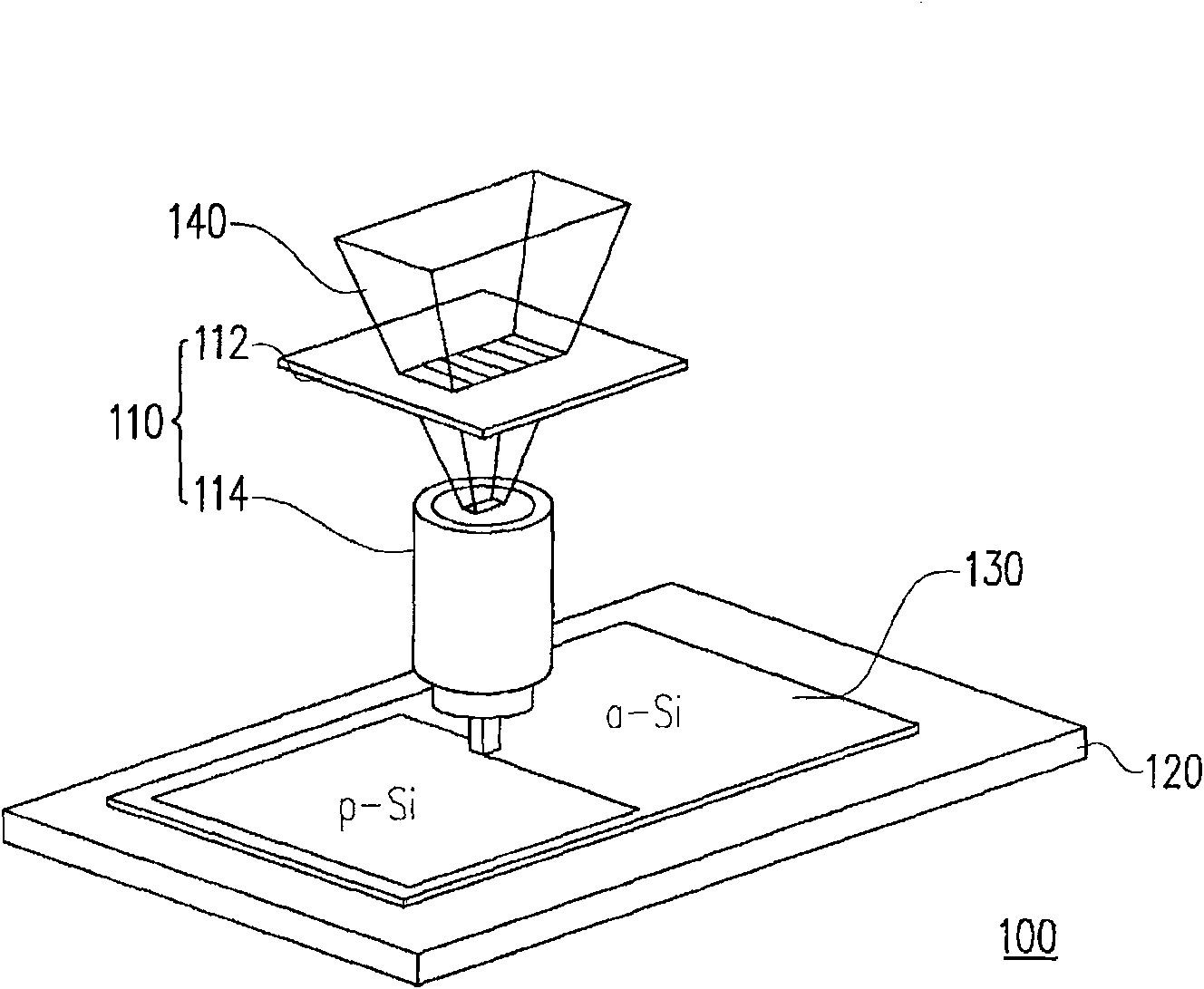
[0020] image 3 is a schematic flowchart of a method for forming a polysilicon layer according to an embodiment of the present invention.

[0021] Please refer to image 3 , firstly, step S300 is performed to form an amorphous silicon layer on the substrate. Then, for example, the substrate formed with the amorphous silicon layer is placed in such as figure 1 Shown is a continuous lateral crystallization laser crystallization device on a substrate stage 120 . Wherein, the material of the substrate is, for example, an inorganic transparent material (such as: glass, quartz, or other suitable materials, or a combination of the above), an organic transparent material (such as: polyolefins, polyols, polyalcohols, polyesters, or combination of the above. In this embodiment, the material of the substrate is glass as an example, but the invention is not limited thereto. The method for forming the amorphous silicon layer is, for example, chemical vapor deposition, inkjet method, ...


PUM

PropertyMeasurementUnit
widthaaaaaaaaaa
widthaaaaaaaaaa
widthaaaaaaaaaa

Abstract

A mask comprises a main shading pattern and a plurality of groups of micro shading patterns. The main shading pattern is used for defining a plurality of strip light transmission slits, wherein the extension directions of the light transmission slits are substantially same. The plurality of groups of micro shading patterns are connected with the main shading pattern, each micro shading pattern is positioned inside one of the light transmission slits, each group of micro shading patterns comprises a plurality of shading patterns, and the extension direction of at least part of the micro shading patterns and the extension direction of light transmission slit form an included angle other than about 90 DEG.

Description

【Technical field】 [0001] The present invention relates to a mask, and in particular to a mask for forming a polysilicon layer. 【Background technique】 [0002] In general components, switches are configured to drive the component. Taking an actively driven display device as an example, a thin film transistor (Thin Film Transistor, TFT) is usually used as a driving switch. Thin film transistors can be classified into amorphous silicon thin film transistors (amorphous silicon TFT) and low temperature polysilicon thin film transistors (Low-Temperature PolySilicon Thin Film Transistor, LTPS-TFT) according to the material of the channel layer. Among them, low-temperature polysilicon thin film transistors have the advantages of low power consumption and high electron mobility compared with amorphous silicon thin film transistors, and thus gradually attract the attention of the market. Therefore, low-temperature polysilicon thin film crystallization technology has been extensively...

Claims


Application Information

Patent Timeline
Patent Type & Authority Patents(China)
IPC IPC(8): H01L21/20H01L21/268H01L21/336H01L21/77H01L21/84B23K26/06B23K26/066
Inventor 孙铭伟
Owner AU OPTRONICS CORP
Why Eureka
Try Eureka