Exposure process for different levels
An exposure method and layered technology, applied in microlithography exposure equipment, photolithography exposure devices, optics, etc., can solve problems such as uncontrollable alignment errors, high mask manufacturing costs, and affecting accuracy
- Summary
- Abstract
- Description
- Claims
- Application Information
AI Technical Summary
Problems solved by technology
Method used
Image
Examples
Embodiment Construction
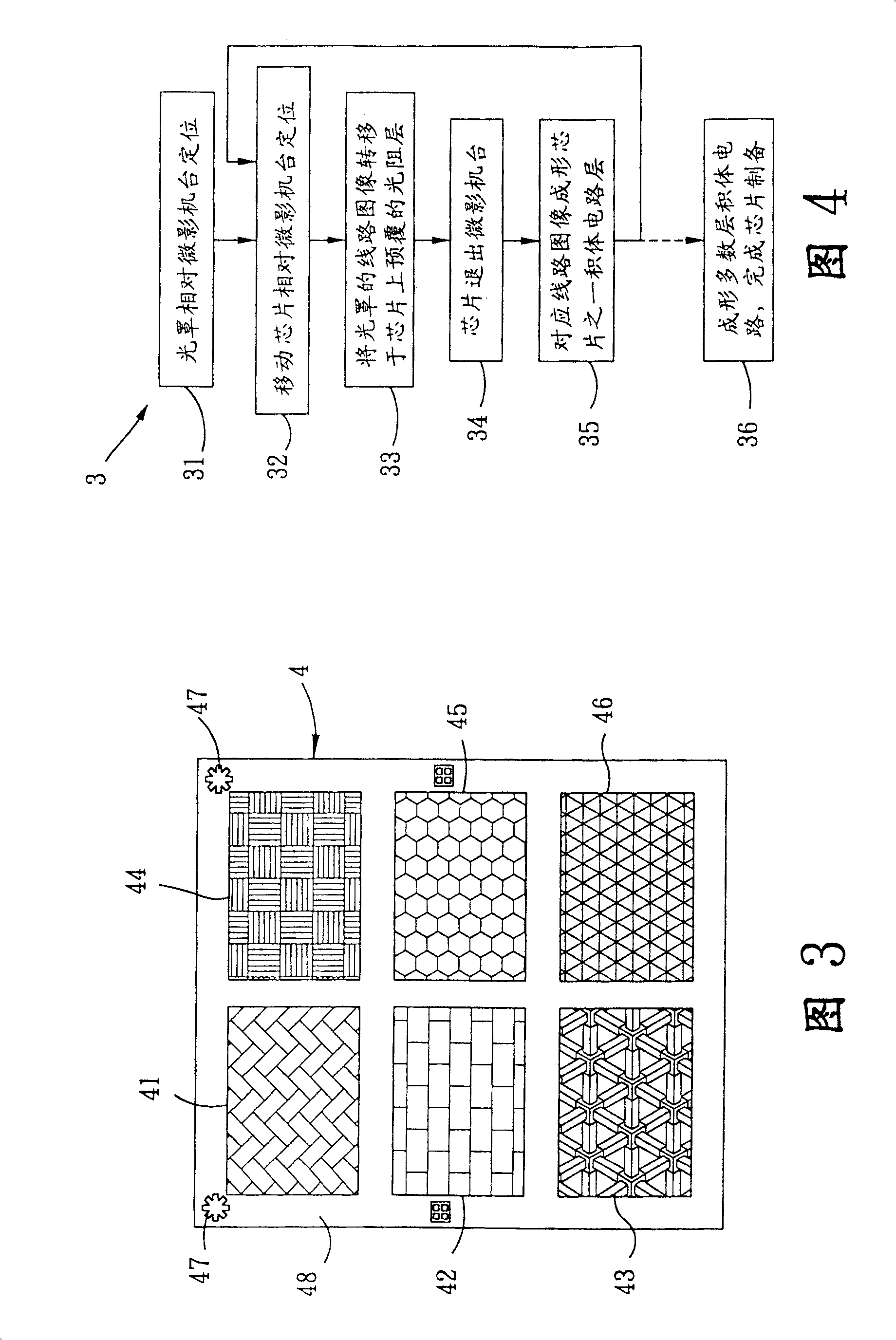
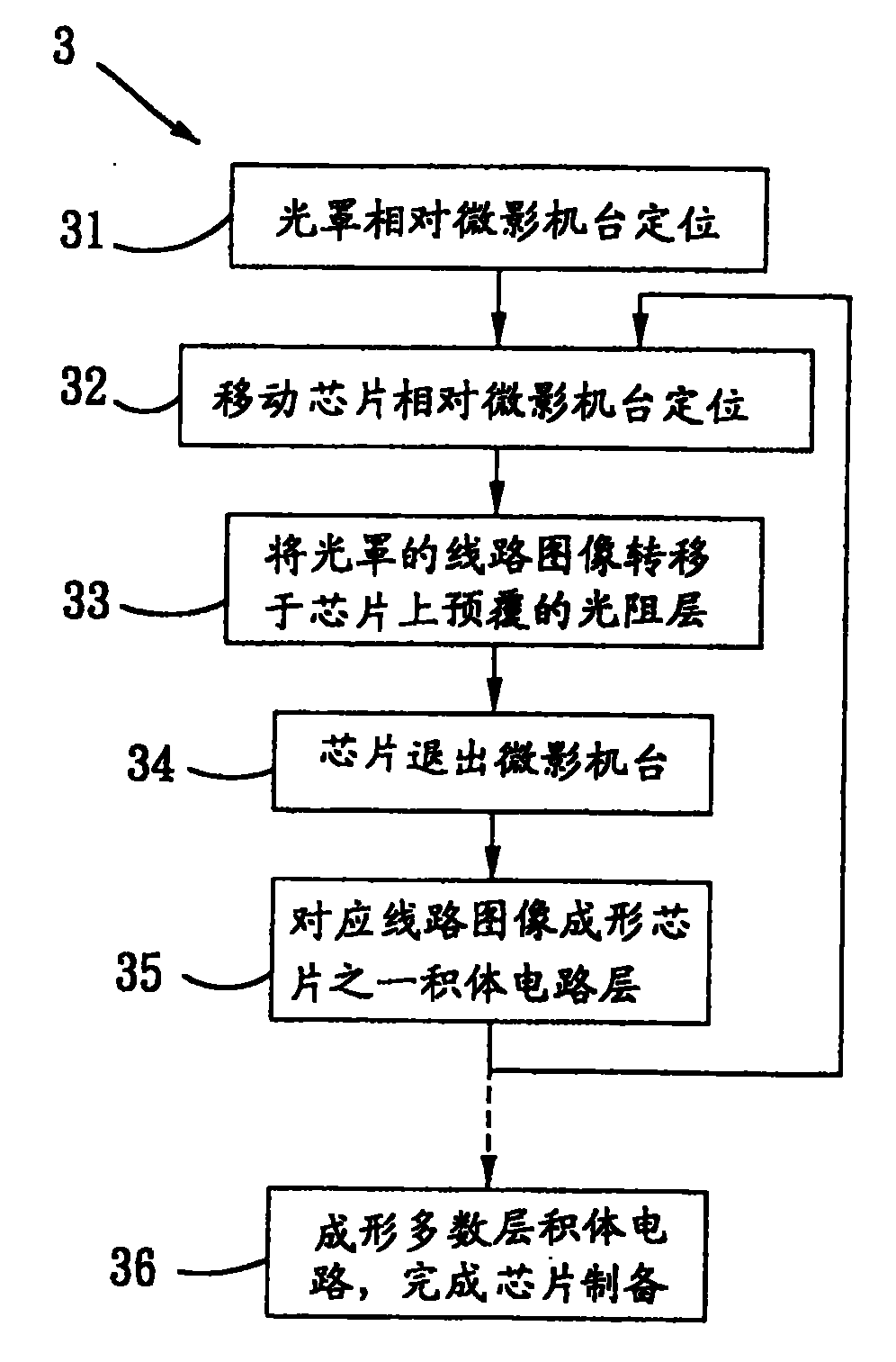
[0055] The different levels of exposure method 3 of the present invention is applicable to the manufacture of many chips in small batches, and a lithography machine is used to perform multi-level exposure on the chips. Each chip has a plurality of integrated circuit layers. In this example, a six-layer integrated circuit will be formed. layer as an example.
[0056] As shown in Figure 3, the photomask 4 used in the present invention can be a binary photomask, or a phase shift photomask, comprising six different circuit images 41, 42, 43, 44, 45, 46, and most of them are arranged around The cross-shaped or rice-shaped positioning mark 47 at the corner (the rice-shaped figure is used as an example in the icon), each line image 41, 42, 43, 44, 45, 46 is designed for each layer of integrated circuits, and the Line images 41, 42, 43, 44, 45, and 46 are also plated with a thickness of about several hundred The chromium film forms a non-transparent region 48, which avoids mutual in...
PUM
 Abstract
Description
Claims
Application Information
 - Generate Ideas
- Intellectual Property
- Life Sciences
- Materials
- Tech Scout
- Unparalleled Data Quality
- Higher Quality Content
- 60% Fewer Hallucinations
Browse by: Latest US Patents, China's latest patents, Technical Efficacy Thesaurus, Application Domain, Technology Topic, Popular Technical Reports.
© 2025 PatSnap. All rights reserved.Legal|Privacy policy|Modern Slavery Act Transparency Statement|Sitemap|About US| Contact US: help@patsnap.com


