Damage-free switching method for main and spare synchronous digital series device timing source
A technology for synchronizing digital series and timing sources, applied in transmission systems, electrical components, etc., can solve the problems of limited scalability, unsuppressible noise, and high requirements for PCB layout and wiring
- Summary
- Abstract
- Description
- Claims
- Application Information
AI Technical Summary
Problems solved by technology
Method used
Image
Examples
Embodiment Construction
[0020] The specific implementation of the method of the present invention will be described in detail below in conjunction with the accompanying drawings.
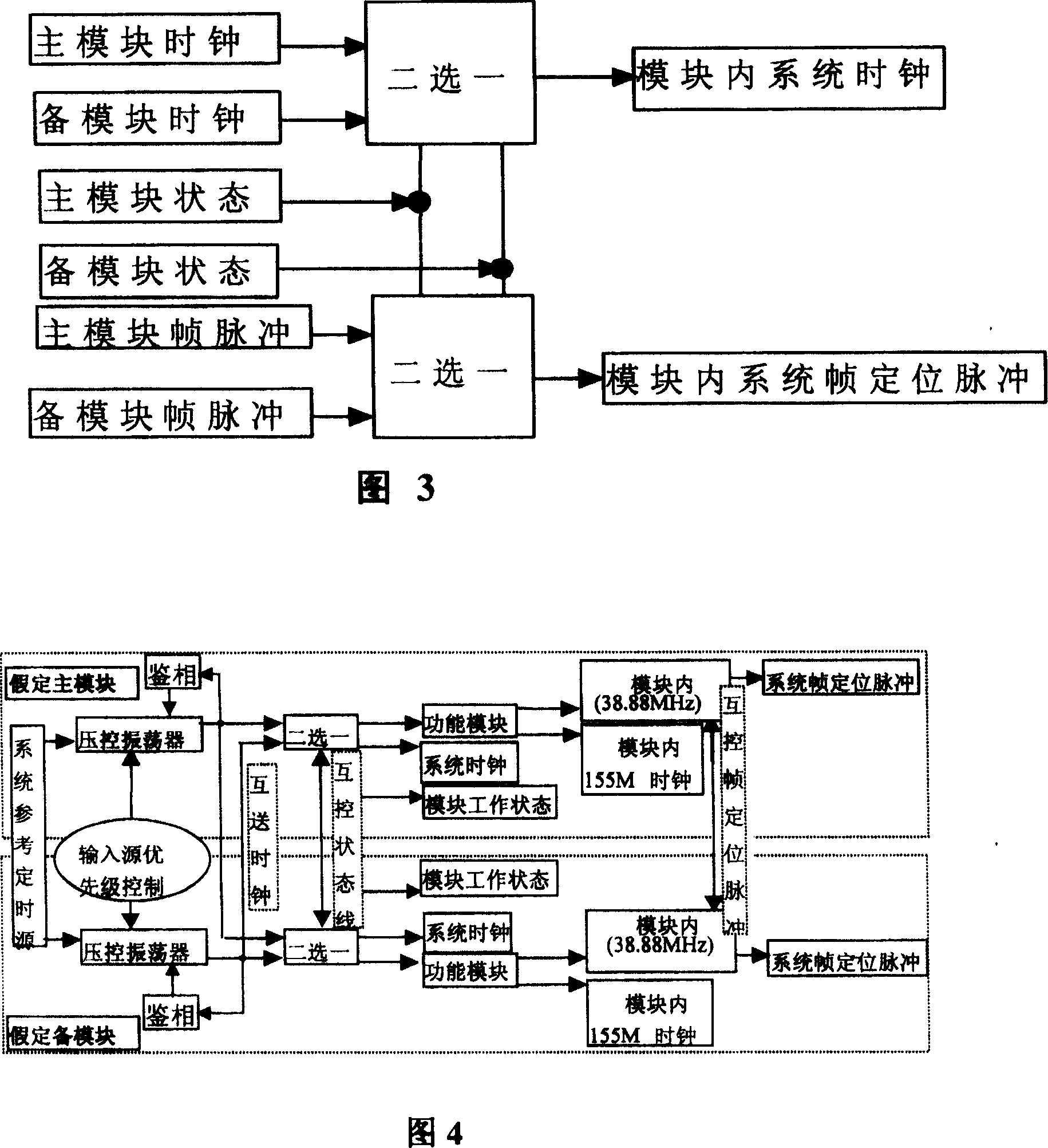
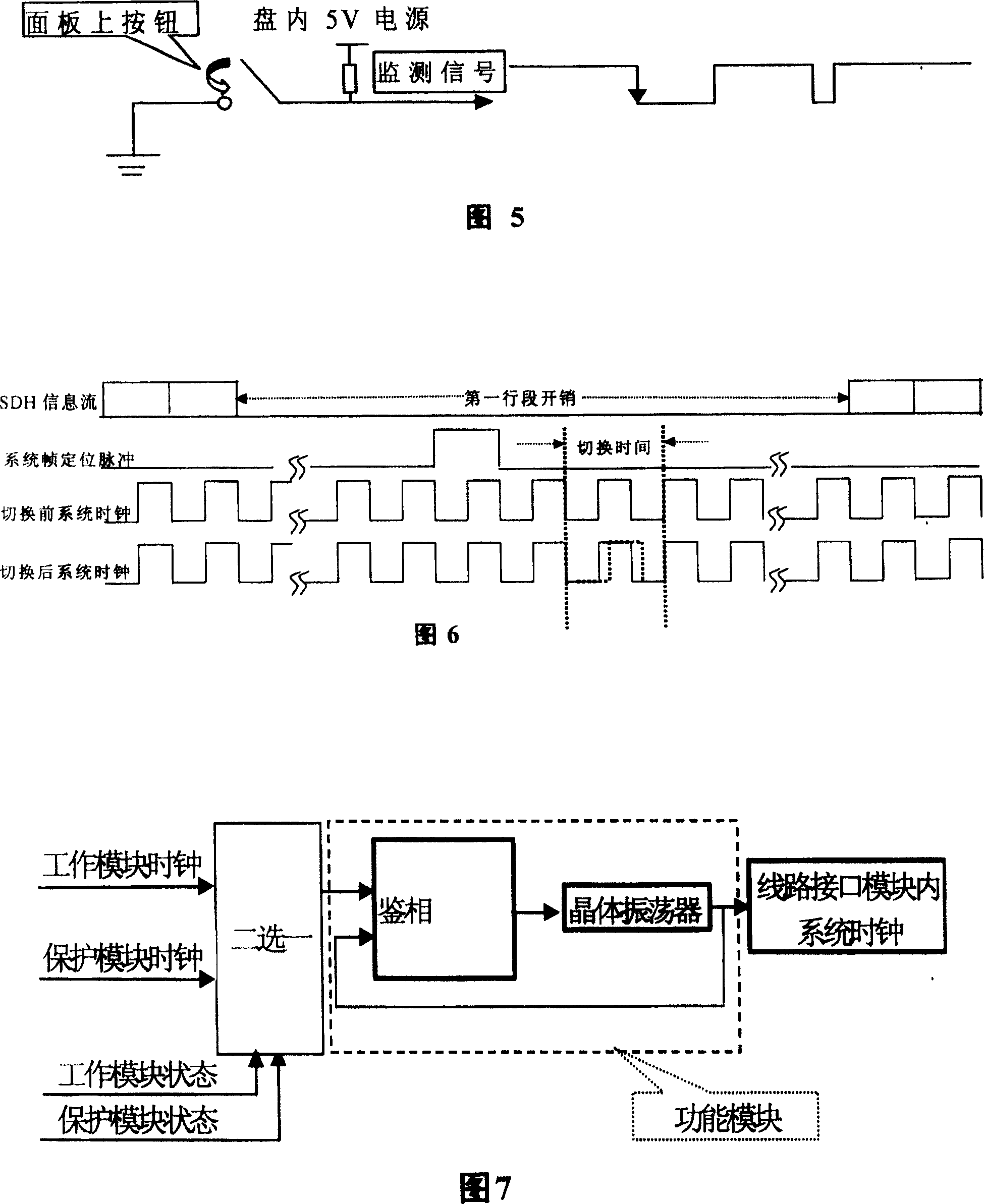
[0021] In the specific implementation process of the method of the present invention, the main and standby timing source modules are used in the following specific ways: first, the logic circuit for selecting one of the two is controlled by the "mutual control status line", and the main module selects the voltage-controlled oscillator in this module (38.88MHz) output clock, the standby module selects the clock sent by the main module; ensure that the output system clock of the two modules is completely consistent with the system frame alignment pulse in the normal main mode; secondly, in the locked mode, due to the main module and The respective voltage-controlled oscillators (38.88MHz) in the standby module track the same timing source, so at the input end of the two-choice logic circuit, the two clock signals have the cha...
PUM
 Abstract
Description
Claims
Application Information
 - R&D
- Intellectual Property
- Life Sciences
- Materials
- Tech Scout
- Unparalleled Data Quality
- Higher Quality Content
- 60% Fewer Hallucinations
Browse by: Latest US Patents, China's latest patents, Technical Efficacy Thesaurus, Application Domain, Technology Topic, Popular Technical Reports.
© 2025 PatSnap. All rights reserved.Legal|Privacy policy|Modern Slavery Act Transparency Statement|Sitemap|About US| Contact US: help@patsnap.com


