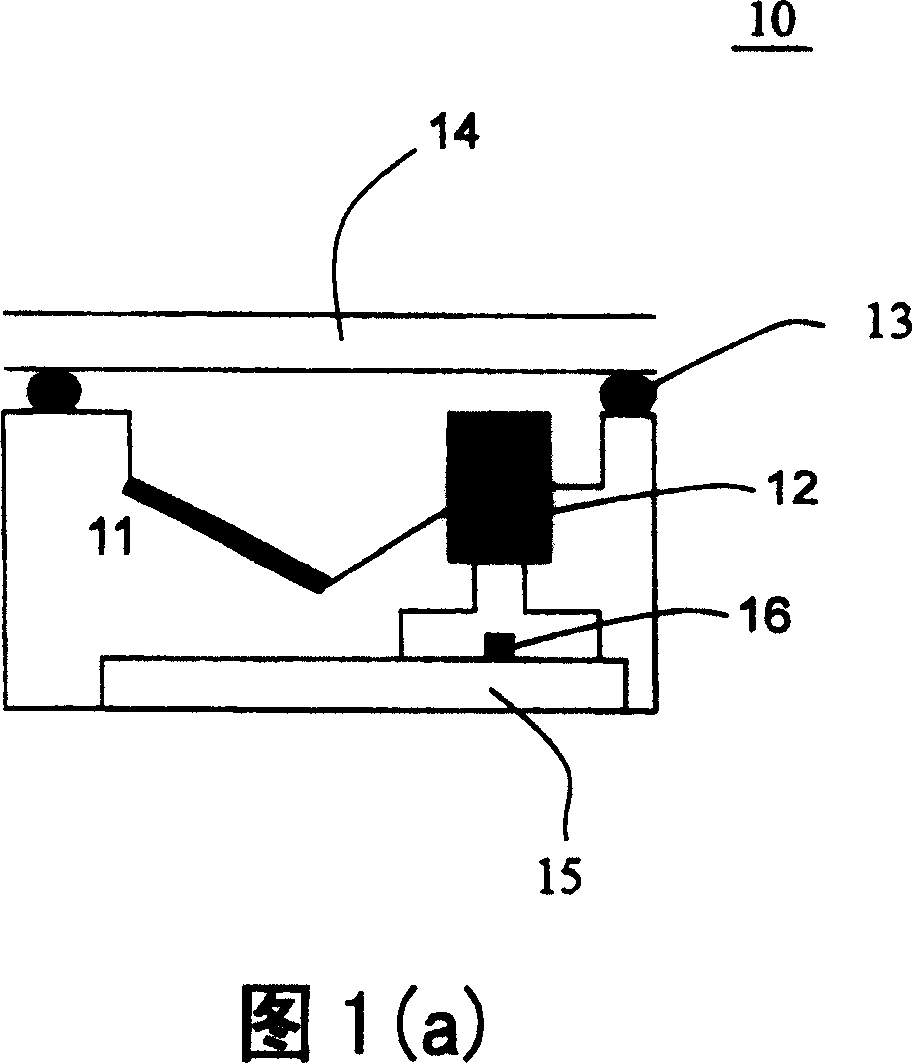
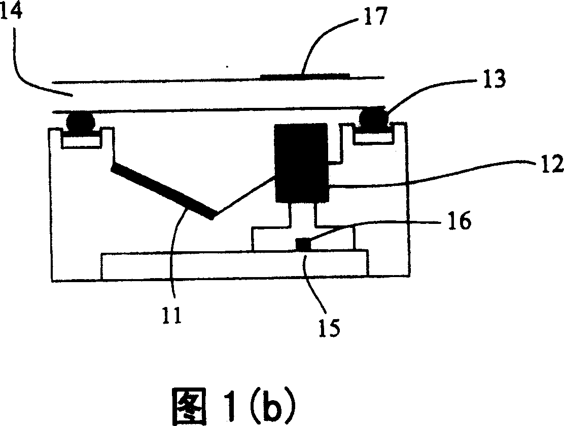
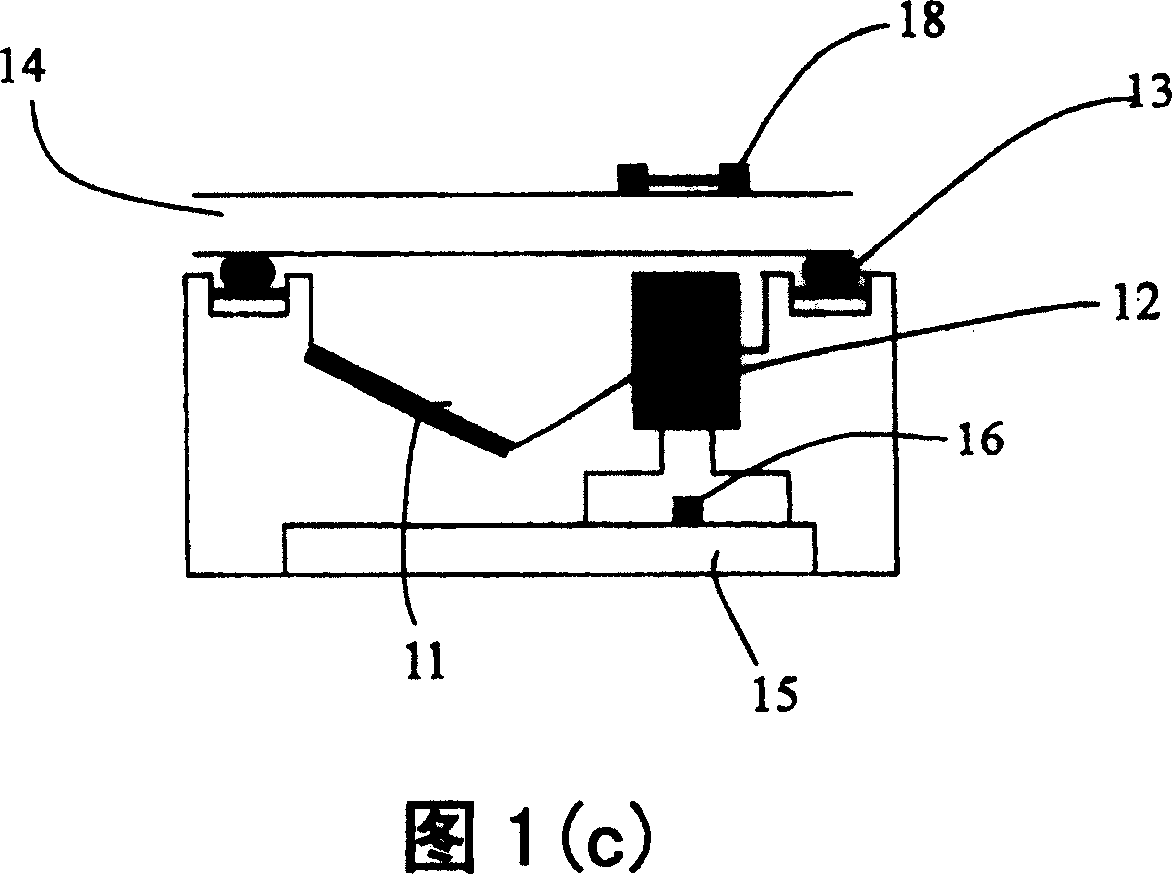
Contact type image scanner with multi-focus and multi resolution ratio
A multi-resolution, contact-type technology, which is applied in the fields of instruments, image communication, optics, etc., can solve the problems that the scanning focal length and resolution are not adjustable, the focal length range of the scanning image is not wide enough, and it can only treat symptoms, etc.
- Summary
- Abstract
- Description
- Claims
- Application Information
AI Technical Summary
Problems solved by technology
Method used
Image
Examples
no. 1 example
[0064] Please refer to FIG. 3( a ), which is a structural diagram of the first embodiment of the contact image scanner with multiple focal lengths and multiple resolutions of the present invention. Wherein, the contact image scanner 30 using contact image sensor (contact image sensor, CIS) technology consists of a first lenticular lens 32, a second lenticular lens 33, a glass 34, a circuit board 35, a first group of photosensitive element arrays 36, and The second group of photosensitive element arrays 37 are jointly packaged in a casing (not shown in the figure).
[0065] In the contact image scanner 30, the first lenticular lens 32 and the second lenticular lens 33 correspond to the first group of photosensitive element arrays 36 and the second group of photosensitive element arrays 37 and are suspended above the two groups of photosensitive element arrays, The glass 34 is suspended above the group of lenticular lenses, and the first group of photosensitive element arrays 36...
no. 2 example
[0073] Please refer to FIG. 5 , which is a structural diagram of a second embodiment of the contact image scanner with multiple focal lengths and multiple resolutions of the present invention. The only difference from the aforementioned first embodiment is that the first group of photosensitive element arrays 56 and the second group of photosensitive element arrays 57 of this embodiment are respectively located on different first circuit boards 55 and second circuit boards 55', The first circuit board 55 and the second circuit board 55' are connected by connectors 51 and 51'.
[0074] Same as the first embodiment, the second photosensitive element array 57 composed of a plurality of second photosensitive elements can be located at the front end or the tail end of the first photosensitive element array 56 composed of a plurality of first photosensitive elements, as long as the two groups The array can be arranged in a single row, as shown in FIG. 4 .
[0075] The focal length ...
no. 3 example
[0080] The structure of the third embodiment of the contact image scanner with multiple focal lengths and multiple resolutions of the present invention is similar to that of the second embodiment, but the only difference is that the first group of photosensitive element arrays 56 and the second Although the groups of photosensitive element arrays 57 are respectively located on different circuit boards, the second group of photosensitive element arrays 57 composed of a plurality of second photosensitive elements and the first group of photosensitive element arrays 56 composed of a plurality of first photosensitive elements are connected to each other. Arranged in a parallel manner; as shown in Figure 6, the length of the second group of photosensitive element arrays 57 can be made according to the requirements of the scanned object, and its position relative to the X axis can also be defined according to the designer's preference, as The map can be at position 1, position 2, pos...
PUM
 Abstract
Description
Claims
Application Information
 - R&D
- Intellectual Property
- Life Sciences
- Materials
- Tech Scout
- Unparalleled Data Quality
- Higher Quality Content
- 60% Fewer Hallucinations
Browse by: Latest US Patents, China's latest patents, Technical Efficacy Thesaurus, Application Domain, Technology Topic, Popular Technical Reports.
© 2025 PatSnap. All rights reserved.Legal|Privacy policy|Modern Slavery Act Transparency Statement|Sitemap|About US| Contact US: help@patsnap.com


