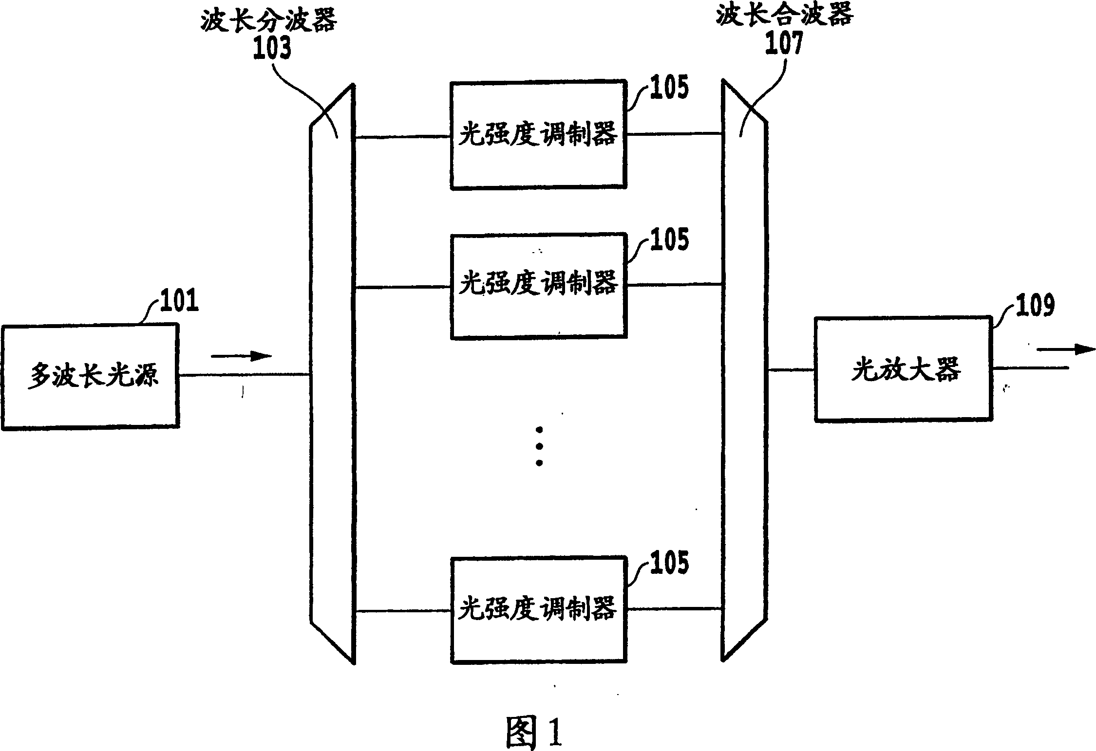
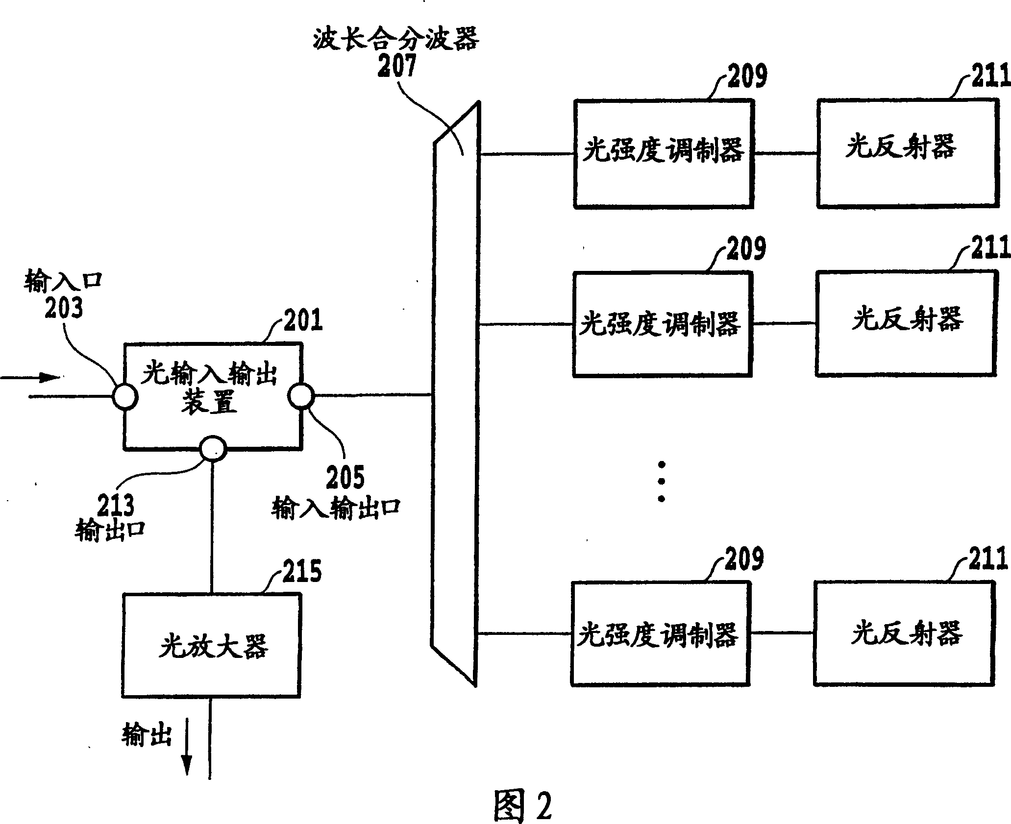
Optical modulating device
A technology of light modulation device and light intensity modulator, which is applied in optics, optical fiber transmission, nonlinear optics, etc., and can solve the problem of large reflected light value, etc.
- Summary
- Abstract
- Description
- Claims
- Application Information
AI Technical Summary
Problems solved by technology
Method used
Image

Examples
Embodiment 1
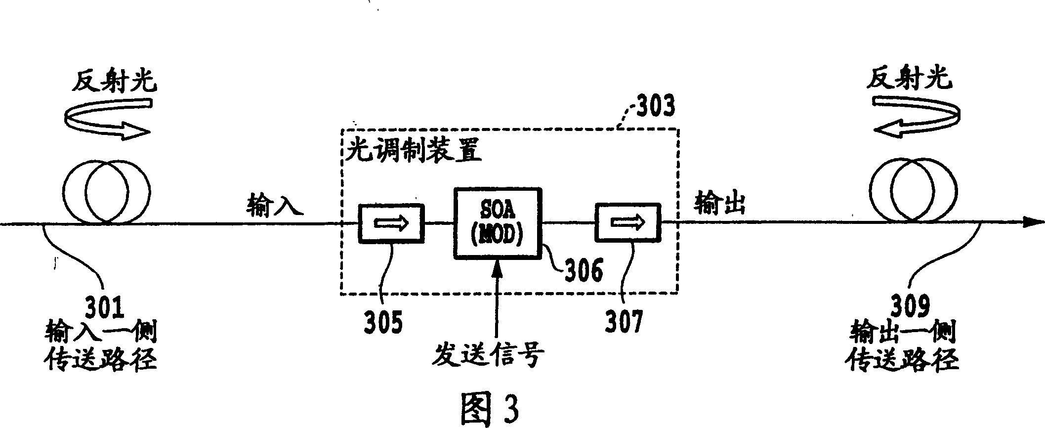
[0045] The first embodiment of the present invention adopts a method of inserting optical isolators every other time into a transmissive optical modulation device including a semiconductor optical amplifier (SOA) connected in multiple stages, and at the same time, it is achieved by reducing the influence of reflected light. The result is an embodiment with stable amplification function and reduced cost. Before describing a specific configuration example of this embodiment, the principle will be explained.
[0046]
[0047] Fig. 7 is a diagram illustrating reflected light when multiple SOAs are connected in multiple stages. In this multi-stage connection structure, in order to make it function as an optical modulation device, although it is necessary to either use one of the SOA to be used as an optical intensity modulator or insert an external modulator, here, In order to simplify the description of reflected light, it is assumed that all SOAs only function as optical amplifiers....
Embodiment 2
[0061] 12A-12C are diagrams illustrating the structure of the light modulation device according to the second embodiment of the present invention. This embodiment corresponds to a modification of the first embodiment, and is applied to the three SOA S constituting the optical amplifier 1 , S 2 , S 3 A light intensity modulator M is inserted between any of them.
[0062] Figure 12A is the optical isolator O 1 , O 2 The light intensity modulator M is inserted in the section of. Here, although it is shown to the first and second SOA S 1 , S 2 2nd optical path (optical connection device) between x 2 The example where the light intensity modulator M is inserted, but it can also be added to the 3rd SOA S 3 4th optical path between output terminal and x 4 Insert the light intensity modulator M inside. However, in this case, it is necessary to use SOA S that can handle the last level 3 A light intensity modulator M with amplified light power.
[0063] In the structure of Figure 12A, from ...
Embodiment 3
[0067] The optical modulation device of the third embodiment of the present invention is made such that in the device configuration having the bidirectional optical amplifier shown in FIG. 4, the numerical limitation of the gain of the amplifier can be adopted as described later, thereby reducing A device that realizes a stable amplification function under the influence of the reflected light on the end face of the bidirectional optical amplifier. Hereinafter, the numerical limitation of the amplifier gain of the present invention will be described.
[0068]
[0069] As shown in FIG. 4, there are two reflected lights from both ends of the bidirectional optical amplifiers 409 and 415, one reflected light 1 and modulated light, and the other reflected light 2 travels in the same direction as the continuous light. The continuous light becomes modulated light due to intensity modulation. Since the reflected light 2 has to go through the same path as the continuous light, the reflecte...
PUM
| Property | Measurement | Unit |
|---|---|---|
| reflectance | aaaaa | aaaaa |
Abstract
Description
Claims
Application Information
 - R&D
- Intellectual Property
- Life Sciences
- Materials
- Tech Scout
- Unparalleled Data Quality
- Higher Quality Content
- 60% Fewer Hallucinations
Browse by: Latest US Patents, China's latest patents, Technical Efficacy Thesaurus, Application Domain, Technology Topic, Popular Technical Reports.
© 2025 PatSnap. All rights reserved.Legal|Privacy policy|Modern Slavery Act Transparency Statement|Sitemap|About US| Contact US: help@patsnap.com