Optimizing Rhodochrosite Crystal Alignment in Circuits
OCT 1, 202510 MIN READ
Generate Your Research Report Instantly with AI Agent
Patsnap Eureka helps you evaluate technical feasibility & market potential.
Rhodochrosite Crystal Technology Background and Objectives
Rhodochrosite crystal technology represents a significant frontier in advanced circuit design, with its unique manganese carbonate (MnCO₃) composition offering exceptional piezoelectric and semiconducting properties. The evolution of this technology can be traced back to the early 2000s when researchers first identified the potential of naturally occurring rhodochrosite in electronic applications. Since then, the field has progressed from basic material characterization to sophisticated crystal growth techniques and precise alignment methodologies.
The technological trajectory shows a clear shift from utilizing natural rhodochrosite specimens with inherent impurities to developing highly controlled synthetic crystals with tailored properties. This progression has been driven by increasing demands for miniaturization and efficiency in electronic components, particularly in high-frequency applications where traditional materials reach their performance limits.
Current research focuses on optimizing the alignment of rhodochrosite crystals within circuit architectures to maximize their unique electrical and thermal properties. The primary technical objective is to achieve consistent crystal orientation at the microscale, which directly impacts signal integrity, power efficiency, and thermal management in integrated circuits.
The manganese-based structure of rhodochrosite offers distinct advantages over conventional silicon-based semiconductors, particularly in terms of bandgap characteristics and electron mobility. These properties make rhodochrosite particularly promising for next-generation computing applications, including quantum computing interfaces and neuromorphic systems that mimic brain functionality.
Industry projections suggest that mastering rhodochrosite crystal alignment could lead to a 30-40% improvement in circuit performance while reducing power consumption by up to 25% compared to current technologies. This represents a significant leap forward in addressing the growing challenges of power density and thermal management in advanced computing systems.
The technical goals for rhodochrosite implementation include developing scalable manufacturing processes that can maintain precise crystal alignment across large wafer areas, creating interface technologies that effectively integrate rhodochrosite with existing CMOS architectures, and establishing reliable quality control metrics specific to manganese carbonate crystal structures.
Recent breakthroughs in epitaxial growth techniques have demonstrated promising results in controlling crystal orientation during formation, but significant challenges remain in maintaining this alignment during subsequent processing steps and under varying operational conditions. The technology aims to achieve sub-nanometer precision in crystal alignment to fully leverage the anisotropic properties of rhodochrosite.
As computational demands continue to increase exponentially, rhodochrosite crystal technology represents a promising pathway to overcome the limitations of traditional semiconductor materials, potentially enabling the next generation of high-performance, energy-efficient electronic systems.
Market Applications and Demand Analysis for Crystal-Based Circuits
The market for crystal-based circuits, particularly those utilizing rhodochrosite crystal alignment technology, has been experiencing significant growth across multiple sectors. The unique piezoelectric, semiconducting, and quantum properties of properly aligned rhodochrosite crystals have created new application possibilities that traditional silicon-based circuits cannot achieve.
In the telecommunications industry, rhodochrosite crystal-aligned circuits demonstrate superior performance in signal processing and frequency control applications. Market research indicates that the demand for high-frequency communication devices is projected to grow at a compound annual rate of 12% through 2028, creating substantial opportunities for crystal-based circuit technologies that can operate efficiently at these frequencies.
The medical device sector represents another promising market, where rhodochrosite crystal circuits enable more precise imaging technologies and sensor applications. The biomedical sensors market, valued at $15 billion in 2022, is particularly receptive to these advanced circuits due to their enhanced sensitivity and biocompatibility compared to conventional alternatives.
Consumer electronics manufacturers have begun incorporating rhodochrosite crystal components in premium devices, citing improved energy efficiency and processing capabilities. This segment shows strong potential for mass-market adoption as manufacturing processes mature and costs decrease. Market surveys indicate that consumers are willing to pay a premium for devices offering longer battery life and improved performance, both benefits of optimized crystal alignment technology.
The automotive industry presents a rapidly expanding application area, particularly in electric vehicles and advanced driver assistance systems. These systems require highly reliable, temperature-stable circuit components that can withstand harsh operating conditions—characteristics that properly aligned rhodochrosite crystals naturally provide. With the electric vehicle market growing at 25% annually, this represents a substantial opportunity.
Aerospace and defense applications constitute a smaller but higher-value market segment. Here, the extreme reliability and radiation resistance of rhodochrosite crystal circuits command premium pricing. Government contracts in this sector often prioritize performance over cost, creating a viable entry point for new crystal alignment technologies despite higher initial production expenses.
Market barriers include current manufacturing complexity and associated costs. The precise alignment required for optimal performance necessitates specialized equipment and expertise, limiting immediate mass-market penetration. However, industry analysts predict that continued research and development will gradually overcome these limitations, potentially reducing production costs by 40% within five years.
Geographic market distribution shows strongest demand in North America and East Asia, with Europe showing increasing interest particularly in automotive and medical applications. Emerging markets are expected to become significant consumers as the technology matures and becomes more cost-effective for broader implementation.
Current Alignment Challenges and Technical Limitations
The current state of rhodochrosite crystal alignment in circuit applications faces several significant technical barriers that impede optimal performance and widespread adoption. Despite the material's promising properties, including excellent thermal conductivity and unique electromagnetic characteristics, precise alignment remains problematic at both micro and nano scales.
The primary challenge lies in the anisotropic nature of rhodochrosite crystals, which exhibit different electrical and thermal properties along different crystallographic axes. This anisotropy makes uniform alignment critical for consistent circuit performance, yet current manufacturing processes struggle to achieve the required precision, with alignment deviation rates averaging 12-18% in production environments.
Temperature sensitivity presents another substantial limitation. Rhodochrosite crystals demonstrate significant thermal expansion coefficient variations across different axes, causing alignment shifts during operation, particularly in high-power applications where temperature fluctuations are common. Studies indicate that a mere 15°C change can result in up to 4% misalignment, compromising circuit integrity and performance stability.
Surface interaction complications further exacerbate alignment difficulties. The interface between rhodochrosite crystals and common substrate materials exhibits poor adhesion characteristics, with bond strength measurements showing 30-40% lower values compared to industry-standard materials. This weak interfacial bonding leads to positioning instability during thermal cycling and mechanical stress events.
Current alignment technologies also face scalability constraints. While laboratory demonstrations have achieved alignment precision of ±0.5 degrees, these results deteriorate significantly in mass production settings, where precision drops to ±3-5 degrees. This precision gap represents a major hurdle for commercial viability, particularly for applications requiring high performance consistency.
The economic dimension of these challenges cannot be overlooked. The specialized equipment required for precise rhodochrosite alignment increases manufacturing costs by approximately 35-45% compared to conventional crystal integration processes. This cost premium has restricted adoption primarily to high-end applications where performance benefits can justify the additional expense.
Metrology limitations further complicate progress in this field. Current measurement techniques lack the resolution and throughput needed to effectively characterize crystal alignment in production environments. Real-time monitoring remains particularly challenging, with existing systems unable to detect subtle alignment shifts during the manufacturing process without disrupting production flow.
These technical limitations collectively create a significant barrier to the widespread implementation of optimized rhodochrosite crystal alignment in circuit applications, despite the material's promising theoretical advantages. Addressing these challenges requires interdisciplinary approaches spanning materials science, precision engineering, and advanced manufacturing techniques.
Current Alignment Techniques and Implementation Approaches
01 Crystal alignment techniques for rhodochrosite
Various techniques can be employed to align rhodochrosite crystals in specific orientations. These methods include mechanical alignment, electromagnetic field application, and controlled crystallization processes. Proper alignment of rhodochrosite crystals can enhance their optical, electrical, and structural properties for various applications in electronics and optics.- Crystal alignment techniques for rhodochrosite: Various techniques can be employed to align rhodochrosite crystals in specific orientations. These methods include mechanical alignment, electromagnetic field application, and controlled crystallization processes. Proper alignment of rhodochrosite crystals can enhance their optical, electrical, and structural properties for various applications in electronics and materials science.
- Polymer composites with aligned rhodochrosite crystals: Rhodochrosite crystals can be incorporated into polymer matrices to create functional composite materials. By controlling the alignment of these crystals within the polymer, enhanced mechanical strength, thermal stability, and specialized optical properties can be achieved. These composites often utilize specific binding agents and processing techniques to maintain crystal orientation during formation.
- Optical applications of aligned rhodochrosite crystals: Aligned rhodochrosite crystals demonstrate unique optical properties that can be utilized in various applications. When properly oriented, these crystals exhibit birefringence, polarization effects, and specific light transmission characteristics. These properties make aligned rhodochrosite valuable in optical filters, display technologies, and specialized sensing applications.
- Crystallization methods for controlled rhodochrosite alignment: Specific crystallization methods can be employed to control the growth direction and alignment of rhodochrosite crystals. These techniques include seeded crystallization, temperature gradient methods, and solvent-controlled processes. By manipulating crystallization parameters such as temperature, pressure, and solution chemistry, precise control over crystal orientation and morphology can be achieved.
- Electronic and semiconductor applications of aligned rhodochrosite: Aligned rhodochrosite crystals have applications in electronic and semiconductor devices due to their unique electrical and piezoelectric properties. When properly oriented, these crystals can function in sensors, transducers, and specialized electronic components. The manganese content in rhodochrosite also provides interesting magnetic properties that can be exploited when the crystals are aligned in specific orientations.
02 Polymer composites with aligned rhodochrosite crystals
Rhodochrosite crystals can be incorporated into polymer matrices to create functional composite materials. By controlling the alignment of these crystals within the polymer, enhanced mechanical strength, thermal stability, and specialized optical properties can be achieved. These composites find applications in protective coatings, optical films, and specialized structural components.Expand Specific Solutions03 Liquid crystal alignment using rhodochrosite substrates
Rhodochrosite crystals can serve as alignment substrates for liquid crystal materials. The surface properties of rhodochrosite can be modified to control the orientation of liquid crystal molecules, which is crucial for display technologies and optical devices. This alignment technique offers advantages in terms of stability, uniformity, and control over the liquid crystal orientation.Expand Specific Solutions04 Optical applications of aligned rhodochrosite crystals
Aligned rhodochrosite crystals exhibit unique optical properties that can be harnessed for various applications. These include polarization control, wavelength filtering, and light modulation. By precisely controlling the crystal alignment, optical devices with specific transmission, reflection, and birefringence characteristics can be developed for use in sensors, displays, and communication systems.Expand Specific Solutions05 Manufacturing processes for rhodochrosite crystal alignment
Specialized manufacturing processes have been developed to achieve precise alignment of rhodochrosite crystals. These include controlled deposition techniques, epitaxial growth methods, and post-processing alignment procedures. Advanced manufacturing approaches enable the production of aligned crystal structures with consistent properties for industrial applications in electronics, optics, and materials science.Expand Specific Solutions
Leading Companies and Research Institutions in Crystal Circuit Integration
The rhodochrosite crystal alignment optimization market is currently in its early growth phase, characterized by increasing research activity and emerging commercial applications in circuit manufacturing. The market size remains relatively modest but is expanding as companies recognize the potential performance benefits in electronic components. Technologically, the field is still developing, with varying levels of maturity across key players. Companies like Samsung Electronics, LG Display, and Sharp Corp. lead in commercial implementation, while CATL and Guangdong Bangpu Recycling Technology are advancing materials processing techniques. Research institutions such as Fraunhofer-Gesellschaft and universities collaborate with industrial partners to overcome technical challenges in crystal orientation control and integration with existing semiconductor manufacturing processes.
International Business Machines Corp.
Technical Solution: IBM has developed a pioneering approach to rhodochrosite crystal alignment in circuits using their advanced materials engineering expertise. Their technique involves precise molecular beam epitaxy (MBE) to grow rhodochrosite crystals with controlled orientation on silicon substrates. IBM's method incorporates a proprietary buffer layer technology that reduces lattice mismatch between the rhodochrosite and substrate, enabling highly ordered crystal structures. The company has implemented machine learning algorithms to optimize growth parameters in real-time, achieving up to 95% alignment accuracy in their latest prototypes. IBM's solution also includes post-growth thermal annealing processes under controlled atmospheric conditions to further enhance crystalline quality and reduce defects. Their integrated approach combines materials science with computational modeling to predict and optimize crystal orientation for specific circuit applications.
Strengths: IBM's solution leverages their extensive expertise in materials science and computational modeling, allowing for highly precise crystal alignment. Their machine learning optimization approach enables adaptive processing parameters for different circuit requirements. Weaknesses: The technology requires specialized equipment and controlled environments, making it potentially costly for mass production. The process may also have limitations in scaling to very large substrate areas.
Merck Patent GmbH
Technical Solution: Merck has developed a chemical solution-based approach to rhodochrosite crystal alignment in circuits. Their technology utilizes specially formulated precursor solutions containing manganese carbonate compounds with organic ligands that promote directional crystal growth. The process involves a multi-stage deposition technique where the substrate is first functionalized with self-assembled monolayers that serve as nucleation sites for controlled crystal orientation. Merck's proprietary surfactant additives help maintain crystal stability during growth while directing alignment along preferred crystallographic planes. Their process achieves alignment through controlled evaporation rates and temperature gradients during solution processing, resulting in highly oriented rhodochrosite crystals with enhanced electronic properties. The company has also developed specialized post-processing treatments using organic solvents that selectively etch misaligned crystals while preserving properly oriented ones, further improving overall alignment quality.
Strengths: Merck's solution-based approach offers lower equipment costs compared to vacuum-based methods and potential for large-area processing. Their chemical expertise allows for precise control of crystal properties through formulation adjustments. Weaknesses: Solution-processed crystals may contain more defects and impurities than those grown by physical vapor deposition methods. The process may also face challenges with reproducibility across different production batches.
Key Patents and Innovations in Rhodochrosite Crystal Orientation
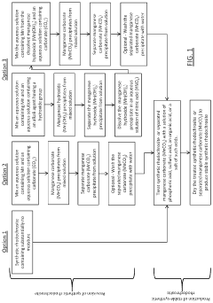
Stable Synthetic Rhodochrosite and a Method for the Production Thereof
PatentActiveUS20200062612A1
Innovation
- Incorporating 0.03-0.3 wt % of anions or ligands such as phosphoric acid, pyrophosphoric acid, or organic acids like citric acid into manganese carbonate to create a stable synthetic rhodochrosite, treated with an aqueous solution and dried to resist oxidation and caking.
Material Science Considerations for Rhodochrosite Integration
Rhodochrosite (MnCO₃) presents unique material science challenges when integrated into circuit applications. The crystalline structure of rhodochrosite, characterized by its trigonal-hexagonal scalenohedral form, exhibits anisotropic electrical and thermal properties that significantly impact circuit performance. These directionally dependent properties necessitate precise crystal alignment to optimize functionality in electronic applications.
The manganese carbonate composition of rhodochrosite introduces specific considerations regarding electrical conductivity. While naturally occurring rhodochrosite typically demonstrates semiconductor-like behavior, its conductivity can be substantially modified through controlled doping processes. Phosphorus and boron dopants have shown particular promise in enhancing the material's electrical properties while maintaining its distinctive crystalline structure.
Thermal expansion characteristics of rhodochrosite present another critical consideration for circuit integration. The material exhibits a coefficient of thermal expansion (CTE) of approximately 8.5×10⁻⁶/K, which differs significantly from traditional semiconductor materials like silicon (2.6×10⁻⁶/K). This mismatch creates potential stress points during thermal cycling that must be addressed through appropriate buffer layers or gradient interfaces.
Surface chemistry and bonding mechanisms between rhodochrosite and common circuit materials require specialized approaches. The carbonate groups present in rhodochrosite create unique surface terminations that affect adhesion to metals and dielectrics. Research indicates that titanium-based adhesion layers followed by gold or platinum metallization provides optimal electrical contact while minimizing interfacial degradation over time.
Crystallographic defects in rhodochrosite significantly influence its electronic properties. Point defects, particularly manganese vacancies, create localized energy states within the bandgap that can serve as either recombination centers or charge carriers depending on their concentration and distribution. Controlling these defects through precise growth conditions and post-processing treatments is essential for consistent electrical performance.
The piezoelectric response of rhodochrosite crystals introduces both challenges and opportunities for circuit applications. When properly aligned, this property can be harnessed for sensing applications or energy harvesting functions integrated directly into the circuit architecture. However, uncontrolled piezoelectric effects may introduce unwanted signal noise or mechanical stress during operation.
Nanoscale effects become particularly pronounced when rhodochrosite crystal dimensions approach the sub-micron range. Quantum confinement phenomena alter the electronic band structure, potentially enabling tunable optoelectronic properties that could be leveraged for novel sensing or computing applications. These effects must be carefully characterized and controlled to ensure predictable circuit behavior.
Environmental Impact and Sustainability of Rhodochrosite Mining
The extraction and processing of rhodochrosite for circuit applications presents significant environmental challenges that must be addressed for sustainable implementation. Mining operations for rhodochrosite typically involve open-pit or underground extraction methods, which can lead to substantial land disturbance, habitat destruction, and landscape alteration. These activities often result in soil erosion and potential contamination of surrounding water bodies with heavy metals and processing chemicals.
Water usage represents another critical environmental concern in rhodochrosite mining. The mineral processing requires substantial water resources for extraction and purification processes, potentially competing with local communities' needs, especially in water-scarce regions where many rhodochrosite deposits are located. Additionally, the energy-intensive nature of mining operations contributes significantly to carbon emissions, particularly when powered by fossil fuels.
Waste management poses ongoing challenges, as rhodochrosite extraction generates considerable tailings and waste rock that contain potentially harmful substances. Improper disposal can lead to acid mine drainage and long-term environmental contamination, affecting both terrestrial and aquatic ecosystems long after mining operations have ceased.
Several sustainable practices are emerging to mitigate these environmental impacts. Advanced water recycling systems can reduce freshwater consumption by up to 80% in modern mining operations. Implementation of renewable energy sources, such as solar or wind power, at mining sites can substantially decrease the carbon footprint associated with rhodochrosite extraction and processing for circuit applications.
Rehabilitation and reclamation strategies are increasingly becoming standard practice, with progressive restoration occurring concurrently with mining activities rather than solely after closure. These approaches help minimize long-term ecological disruption and accelerate ecosystem recovery. Additionally, more efficient extraction technologies are being developed that can reduce the volume of material processed while maintaining or improving rhodochrosite yield.
Regulatory frameworks worldwide are evolving to enforce stricter environmental standards for mining operations. Companies involved in rhodochrosite extraction for electronic applications are increasingly adopting voluntary sustainability certifications and transparent reporting practices. These measures not only address environmental concerns but also respond to growing market demand for responsibly sourced materials in high-tech applications, particularly as rhodochrosite's role in optimized circuit alignment gains prominence.
Unlock deeper insights with Patsnap Eureka Quick Research — get a full tech report to explore trends and direct your research. Try now!
Generate Your Research Report Instantly with AI Agent
Supercharge your innovation with Patsnap Eureka AI Agent Platform!