Liquid discharge head
a liquid discharge head and liquid discharge technology, applied in the direction of printing, other printed circuit details, conductive pattern formation, etc., can solve the problems of increasing the number of resist-layer removal steps and reducing manufacturing efficiency
- Summary
- Abstract
- Description
- Claims
- Application Information
AI Technical Summary
Benefits of technology
Problems solved by technology
Method used
Image

Examples
first example embodiment
[0024]A first example embodiment of the disclosure will be described below with reference to the drawings.
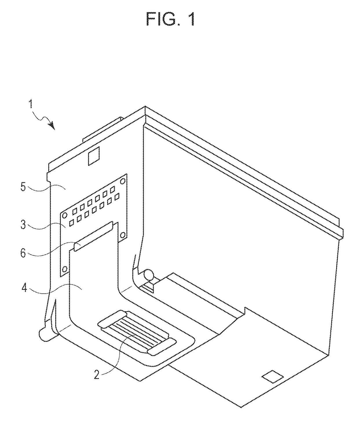
[0025]FIG. 1 is a perspective view of a liquid discharge head 1 to which the first embodiment can be applied. The liquid discharge head 1 includes a liquid discharge substrate (element substrate) 2 that discharges a liquid, an electrical wiring board 4, a printed circuit board 3, and a housing 5. In the electrical wiring board 4 that is capable of transmitting an electric signal, an electric signal path (that is capable of supplying an electric signal) is formed, and the electric signal path applies an electric signal for discharging a liquid to the liquid discharge substrate 2. An electrical-terminal connecting portion 6 is formed at an end of the electrical wiring board 4, and the electrical-terminal connecting portion 6 is used for electrically connect the electrical wiring board 4 and the printed circuit board 3, which includes an external-signal input terminal for receiving...
second example embodiment
[0044]A second embodiment of the disclosure will be described below with reference to the drawings. Note that the basic configuration of the second embodiment is similar to that of the first embodiment, and thus, only characteristic configurations of the second embodiment will be described.
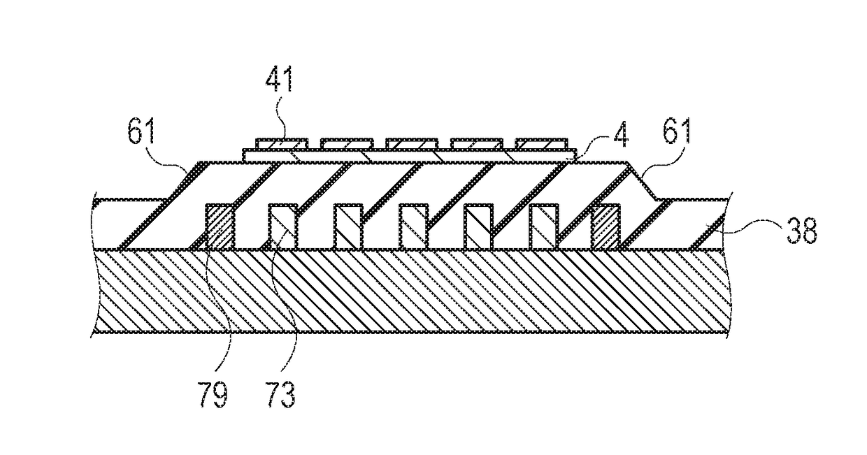
[0045]FIG. 11A is a schematic diagram illustrating a printed circuit board according to the second embodiment, and FIG. 11B is a cross-sectional view taken along line XIB-XIB of FIG. 11A. In the second embodiment, the positions of the inclined surface portions 61 of the resist 38 are spaced away from the bonding position of the electrical wiring board 4 by increasing the width of each of the outermost plated wiring lines 73 among the plated wiring lines 73. In other words, in the second embodiment, the protruding structures 79 are formed integrally with the corresponding outermost plated wiring lines 73. As illustrated in FIGS. 11A and 11B, in the second embodiment, the width of each of plated wir...
third example embodiment
[0052]A third embodiment of the disclosure will be described below with reference to the drawings. Note that the basic configuration of the third embodiment is similar to that of the first embodiment, and thus, only characteristic configurations of the third embodiment will be described.
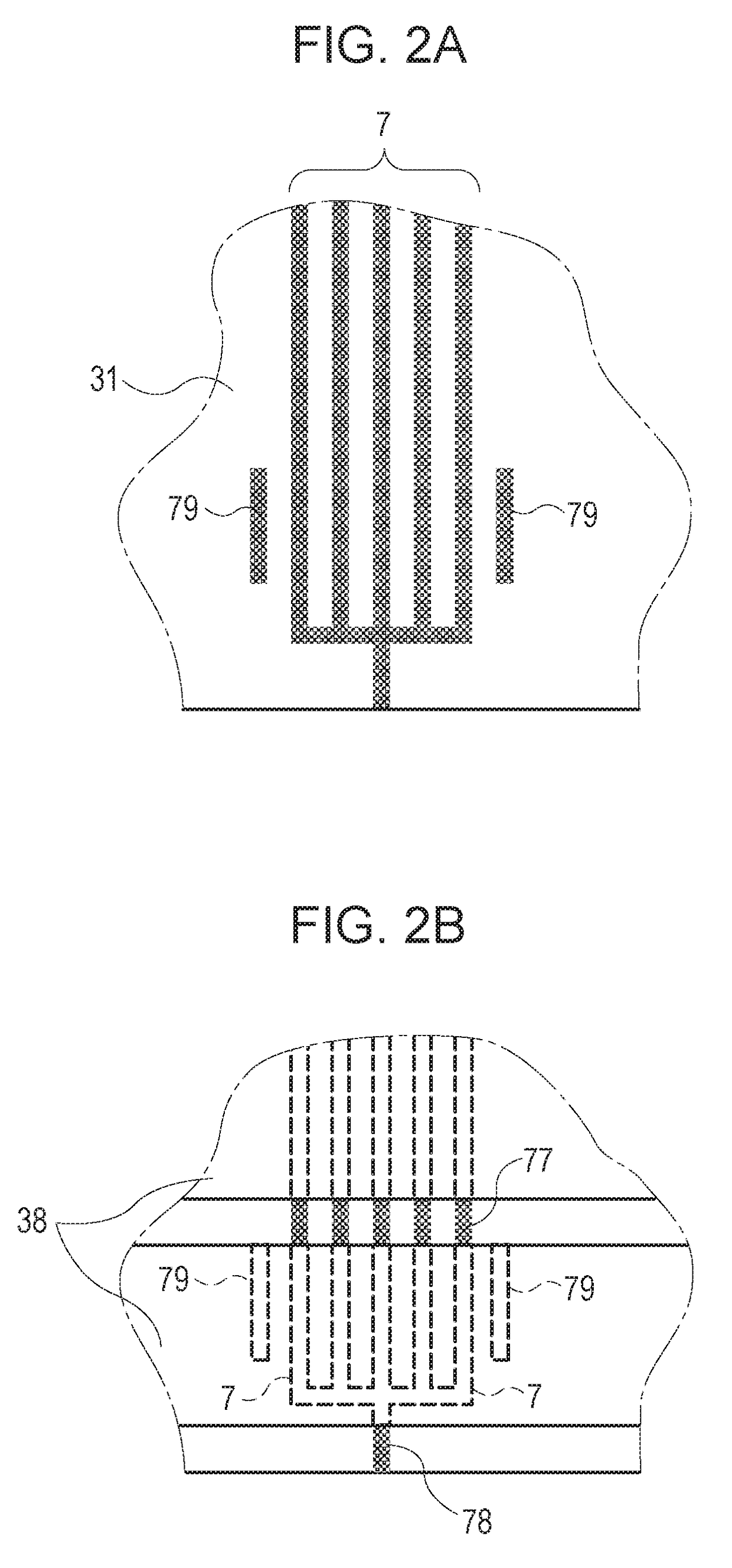
[0053]FIG. 14 is a schematic diagram illustrating a state where the electrical wiring board 4 is bonded to a printed circuit board according to the third embodiment. In the third embodiment, a case will be described in which the array width (A) of the bonding pads 41 of the electrical wiring board 4 is larger than the array width (B) of the plated wiring lines 73. In the case where the array width (A) of the bonding pads 41 of the electrical wiring board 4 is larger than the array width (B) of the plated wiring lines 73, the protruding structures 79 are arranged in such a manner that the arrangement distance (C) of the protruding structures 79 on both sides of the array of the plated wiring lines 73 ...
PUM
 Abstract
Description
Claims
Application Information
 - R&D
- Intellectual Property
- Life Sciences
- Materials
- Tech Scout
- Unparalleled Data Quality
- Higher Quality Content
- 60% Fewer Hallucinations
Browse by: Latest US Patents, China's latest patents, Technical Efficacy Thesaurus, Application Domain, Technology Topic, Popular Technical Reports.
© 2025 PatSnap. All rights reserved.Legal|Privacy policy|Modern Slavery Act Transparency Statement|Sitemap|About US| Contact US: help@patsnap.com