Package substrate and structure

a technology of packaging substrate and package structure, applied in the direction of non-printed electric components of printed circuits, other printed circuit details, non-metallic protective coating applications, etc., can solve the problems of easy warpage of package substrate, reduced product yield, increased overall thickness of package substrate and final package structure, etc., to increase the rigidity of the package substrate, reduce structure, the effect of not increasing the overall thickness of the package substra

Active Publication Date: 2018-02-20
SILICONWARE PRECISION IND CO LTD
View PDF4 Cites 2 Cited by
  • Summary
  • Abstract
  • Description
  • Claims
  • Application Information

AI Technical Summary

Benefits of technology

[0020]Therefore, by providing a thickness difference between the circuit layers, the present invention increases the rigidity of the package substrate so as to reduce warpage of the package substrate. Further, the sum of the thicknesses of the circuit layers can be kept unchanged so as not to increase the overall thickness of the package substrate and structure.

Problems solved by technology

However, during a temperature cycle test of a flip-chip packaging process, warpage easily occurs to the package substrate due to a big CTE (Coefficient of Thermal Expansion) mismatch or asymmetrical heating between the chip and the package substrate.
Consequently, it becomes difficult to form good joints between conductive bumps around an outer periphery of the chip and contacts of the package substrate, thereby reducing the product yield.
However, such an increase in the thickness of the circuit layers results in an increase of the overall thickness of the package substrate as well as the final package structure, thereby hindering miniaturization of electronic products.

Method used


Image

  • Package substrate and structure
  • Package substrate and structure
  • Package substrate and structure

Examples


Embodiment Construction

[0024]The following illustrative embodiments are provided to illustrate the disclosure of the present invention, these and other advantages and effects can be apparent to those in the art after reading this specification.

[0025]It should be noted that all the drawings are not intended to limit the present invention. Various modifications and variations can be made without departing from the spirit of the present invention. Further, terms such as “upper”, “lower” etc. are merely for illustrative purposes and should not be construed to limit the scope of the present invention.

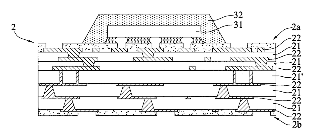
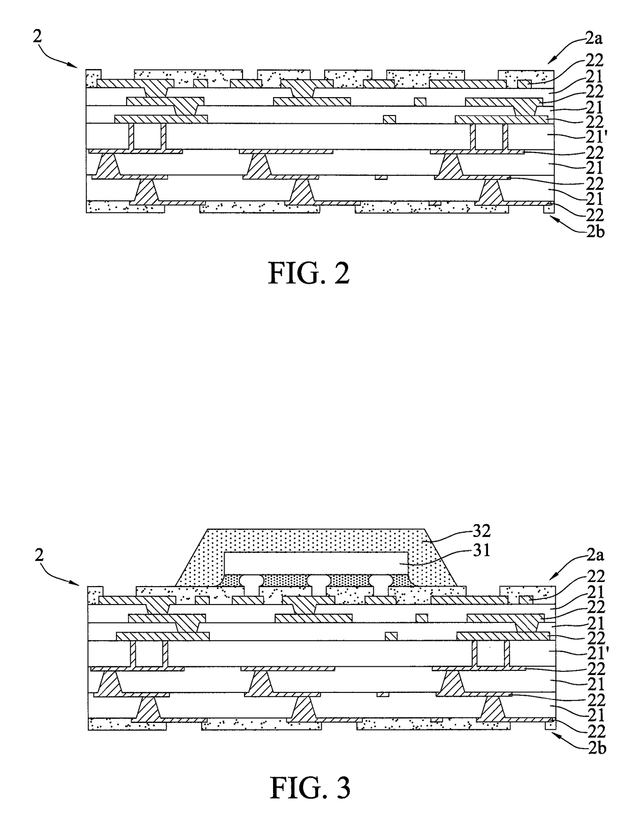
[0026]FIG. 2 is a schematic cross-sectional view of a package substrate of the present invention. Referring to FIG. 2, the package substrate 2 has: a plurality of dielectric layers 21; and a plurality of circuit layers 22 alternately stacked with the dielectric layers 21. At least two of the circuit layers 22 have a difference in thickness. One of the dielectric layers 21 is a core layer 21′ and the circuit layers...


PUM


Abstract

A package substrate is provided, which includes a plurality of dielectric layers and a plurality of circuit layers alternately stacked with the dielectric layers. At least two of the circuit layers have a difference in thickness so as to prevent warpage of the substrate.

Description

CROSS-REFERENCES TO RELATED APPLICATIONS[0001]This application claims under 35 U.S.C. § 119(a) the benefit of Taiwanese Application No. 103105445, filed Feb. 19, 2014, the entire contents of which is incorporated herein by reference.BACKGROUND OF THE INVENTION[0002]1. Field of the Invention[0003]The present invention relates to package substrates and package structures, and more particularly, to a package substrate having a plurality of dielectric layer and a plurality of circuit layers alternately stacked on one another and a package structure having the package substrate.[0004]2. Description of Related Art[0005]Flip-chip technologies facilitate to reduce chip packaging sizes and shorten signal transmission paths and therefore have been widely used for chip packaging. Various types of packages such as chip scale packages (CSPs), direct chip attached (DCA) packages and multi-chip module (MCM) packages can be achieved through flip-chip technologies.[0006]FIG. 1 is a schematic cross-s...

Claims


Application Information

Patent Timeline
Patent Type & Authority Patents(United States)
IPC IPC(8): H05K1/00H05K3/46H05K1/09H05K1/18H05K1/02H05K3/28
CPCH05K3/4644H05K3/284H01L2924/181H01L2924/00012H01L2224/73204H01L2224/16225H01L2224/32225H01L2924/00H05K2203/0369H05K2203/0353H05K2201/20H05K2201/09736H05K2201/0191H05K1/02H05K1/0296H05K1/0298H05K1/181
Inventor LIN, CHANG-FUYAO, CHIN-TSAICHUANG, MING-CHINLIU, KO-CHENGHUANG, FU-TANG
Owner SILICONWARE PRECISION IND CO LTD
Why Eureka
Try Eureka