Apparatus for controlling insulating gate-type semiconductor element, and power conversion apparatus using apparatus for controlling insulating gate-type semiconductor element
a technology of insulating gate-type semiconductor elements and power conversion apparatuses, which is applied in the direction of process and machine control, pulse technique, instruments, etc., can solve the problems of difficult improvement of igbt performance, and achieve the effect of improving the reliability of the power conversion apparatus employing an insulating gate-type semiconductor element that is provided with a plurality of insulating gates
- Summary
- Abstract
- Description
- Claims
- Application Information
AI Technical Summary
Benefits of technology
Problems solved by technology
Method used
Image
Examples
embodiment 1
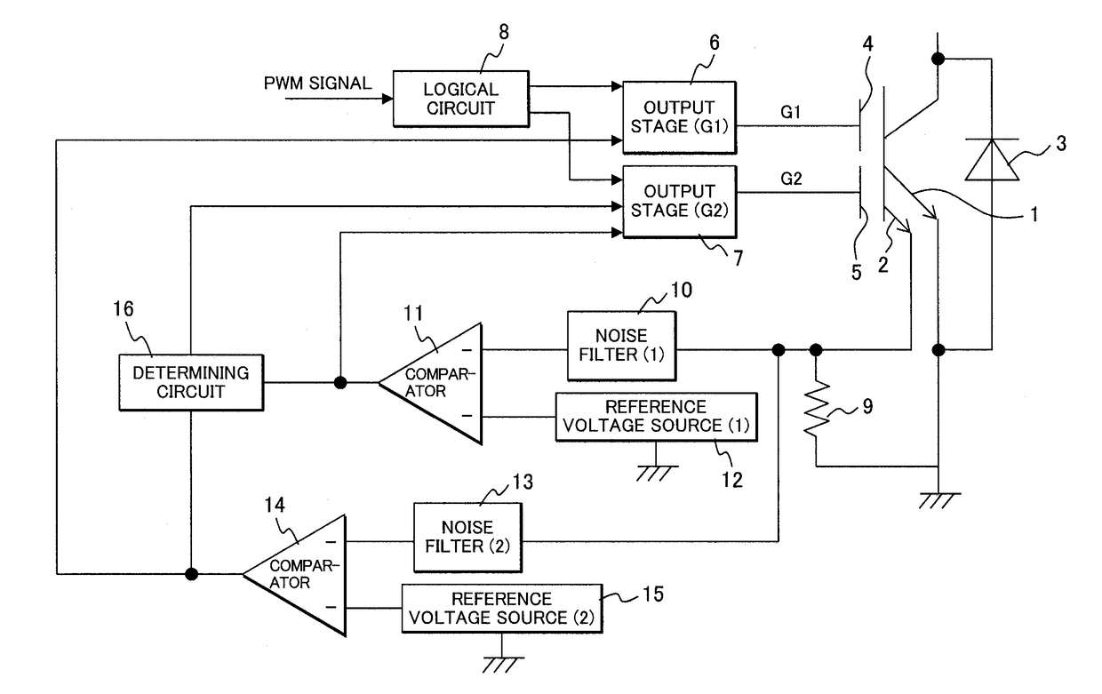
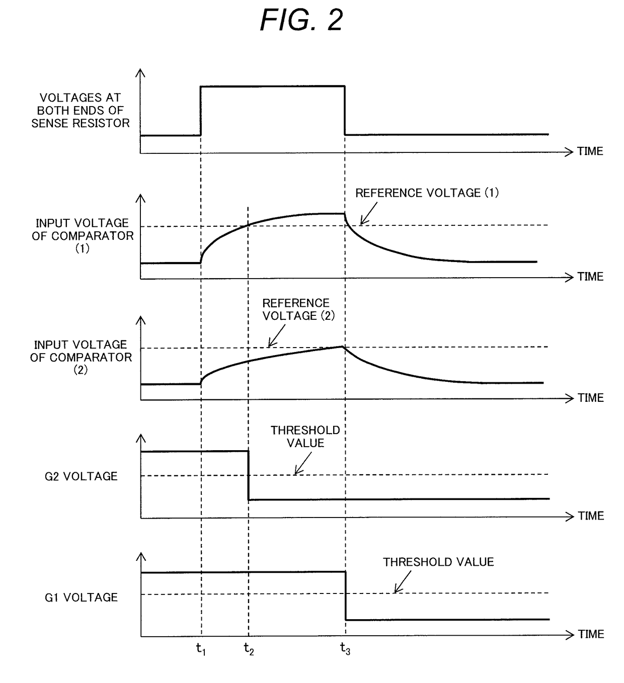
[0037]FIG. 1 is a circuit block diagram of an apparatus for controlling an insulating gate-type semiconductor element, according to a first embodiment of the present invention. This embodiment includes an IGBT 1, a sense IGBT 2, a diode 3, a primary gate (G1) 4, an auxiliary gate (G2) 5, an output stage 6 of a G1 drive circuit that is a first control voltage output circuit supplying a first control voltage to the G1, an output stage 7 of a G2 drive circuit that is a second control voltage output circuit supplying a second control voltage to the G2, a logical circuit 8 receiving a PWM signal and outputting control signals of the G1 and G2, a sense resistor 9, a first noise filter 10, a first comparator 11, a first reference voltage source 12, a second noise filter 13, a second comparator 14, a second reference voltage source 15, and a determining circuit 16 returning the auxiliary gate (G2) 5 to an on-state if an-off signal that is a second comparison result is not outputted from the...
embodiment 2
[0051]FIG. 7 is a circuit block diagram of an apparatus for controlling an insulating gate-type semiconductor element, according to a second embodiment of the present invention. The difference of this embodiment from the first embodiment lies in that the first noise filter 10 and the second noise filter 13 are connected in series. That is, the voltages at the both ends of the sense resistor 9 are inputted to the second noise filter 13 via the first noise filter 10. In the first embodiment, the first noise filter 10 and the second noise filter 13 are connected in parallel, so that the time constant of the second noise filter 13 is set larger than the time constant of the first noise filter 10. On the contrary, in this embodiment, there is no limitation on the time constants of the first noise filter 10 and second noise filter 13 as in the first embodiment.
[0052]In this embodiment, the auxiliary gate (G2) is also turned off at first, whereby the saturation current of the IGBT is reduc...
embodiment 3
[0053]FIG. 8 is a circuit block diagram of an apparatus for controlling an insulating gate-type semiconductor, according to a third embodiment of the present invention. The difference of this embodiment from the first embodiment lies in that the noise filter, the reference voltage source, and the comparator are used one by one.
[0054]Next, the operation of this embodiment will be explained with reference to FIGS. 9 to 11.
[0055]In FIG. 9, if the input voltage of the first comparator exceeds the first reference voltage (t2), the auxiliary gate (G2) is turned off. In this state, the collector current continues to flow. However, the auxiliary gate (G2) is in the off-state, so that the saturation current is reduced and heating of the IGBT is suppressed. Then, if the predetermined time td passes (t3) and the input voltage of the first comparator is kept at a voltage equal to or higher than the reference voltage, the primary gate (G1) is turned off and the IGBT becomes the off-state.
[0056]I...
PUM
 Abstract
Description
Claims
Application Information
 - R&D
- Intellectual Property
- Life Sciences
- Materials
- Tech Scout
- Unparalleled Data Quality
- Higher Quality Content
- 60% Fewer Hallucinations
Browse by: Latest US Patents, China's latest patents, Technical Efficacy Thesaurus, Application Domain, Technology Topic, Popular Technical Reports.
© 2025 PatSnap. All rights reserved.Legal|Privacy policy|Modern Slavery Act Transparency Statement|Sitemap|About US| Contact US: help@patsnap.com


