
Parallelism adjusting device and parallelism adjusting method

a technology of parallelism and adjustment device, which is applied in the direction of measurement device, electronic circuit testing, instruments, etc., can solve the problems of inability to shorten the inspection time per semiconductor, and the semiconductor becomes vulnerable to physical loads, so as to reduce the load on the semiconductor, shorten the cycle time, and increase the operating speed

Active Publication Date: 2017-09-05
HONDA MOTOR CO LTD
View PDF14 Cites 0 Cited by
  • Summary
  • Abstract
  • Description
  • Claims
  • Application Information

AI Technical Summary

Benefits of technology

[0008]Recently, semiconductors are configured with thin layers, and the internal structures thereof are complicated so that the semiconductors become vulnerable to physical loads. Therefore, a probe device needs to be configured so that contact operation is accurately controlled in order to reduce the load caused by weight concentration on the semiconductor when the surface of the semiconductor and the surface of an electrode such as the above-described contact member are in contact with each other. For this reason, the probe device requires elaborate operations so that the operating speed of the probe device is lowered. As a result, there is a problem in that the cycle time as the inspection time per semiconductor cannot be shortened.
[0009]The present invention is for solving the above-described problems and an object thereof is to provide a parallelism adjusting device and a parallelism adjusting method capable of adjusting the parallelism between the surface of the semiconductor and the surface of the electrode by reducing the load on the semiconductor and that is capable of shortening the cycle time by increasing the operating speed.

Problems solved by technology

Recently, semiconductors are configured with thin layers, and the internal structures thereof are complicated so that the semiconductors become vulnerable to physical loads.
As a result, there is a problem in that the cycle time as the inspection time per semiconductor cannot be shortened.

Method used


Image

  • Parallelism adjusting device and parallelism adjusting method
  • Parallelism adjusting device and parallelism adjusting method
  • Parallelism adjusting device and parallelism adjusting method

Examples


first embodiment

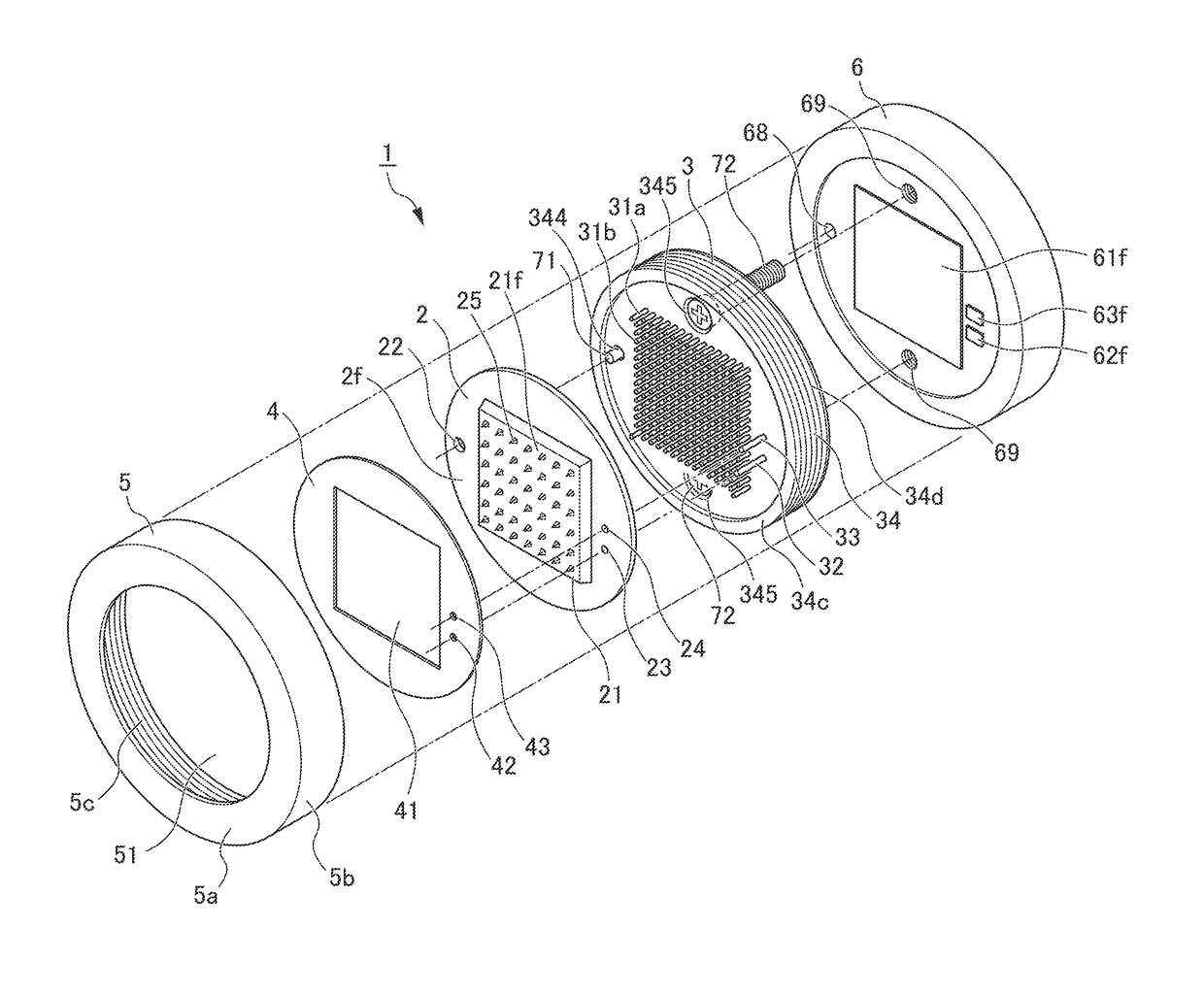
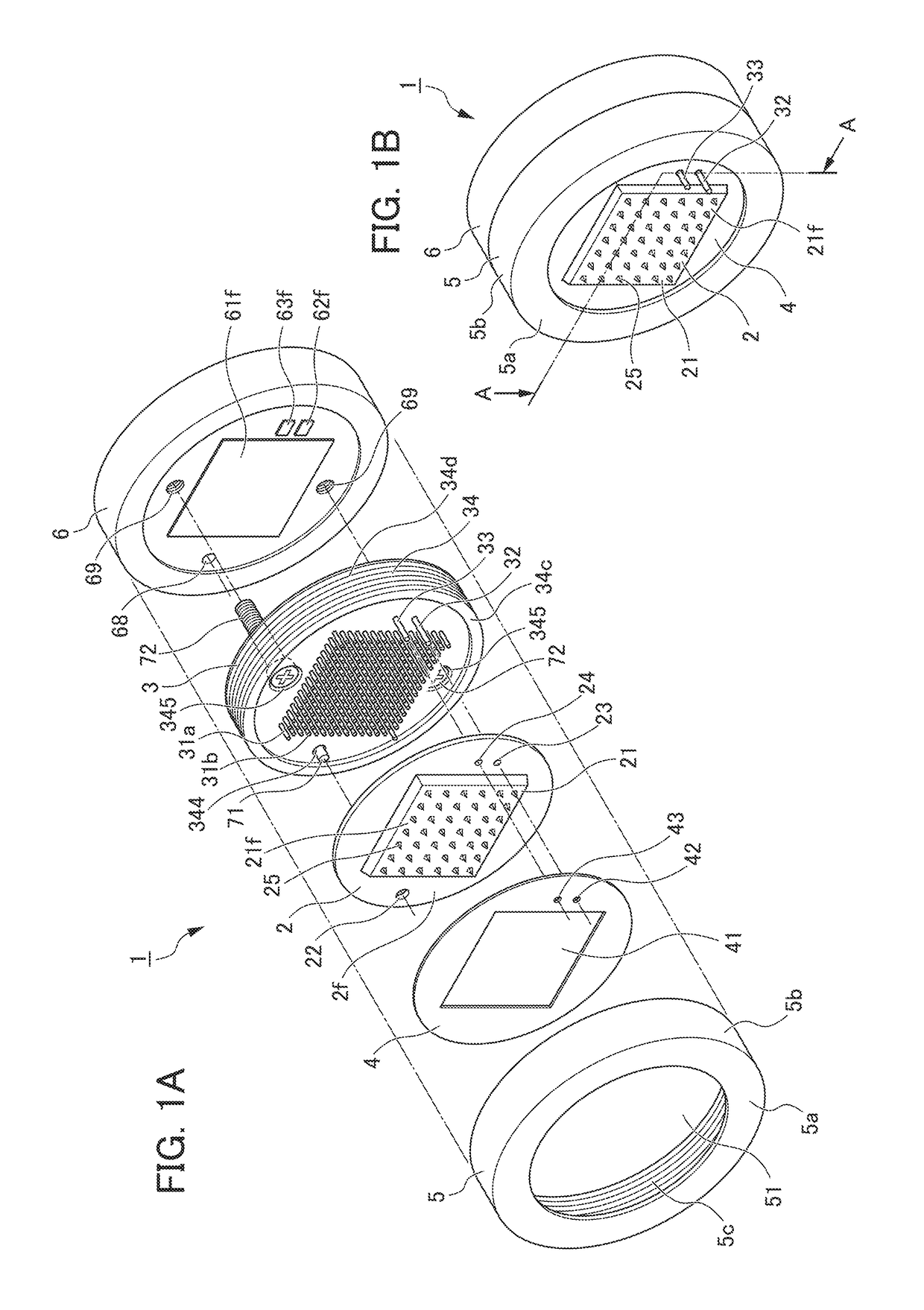
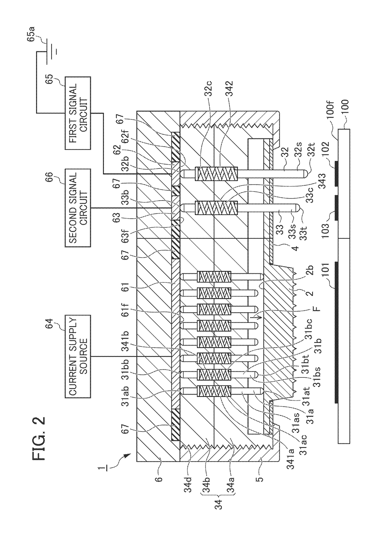
[0027]FIGS. 1A and 1B are perspective views illustrating a schematic configuration of a probe device 1 as a current applying device according to a first embodiment of the present invention, FIG. 1A is an exploded view, and FIG. 1B is an overall view. FIG. 2 is a cross-sectional view of the probe device 1 according to the embodiment taken along line A-A of FIG. 1B. In the cross section taken along line A-A of FIG. 1A, the cutting direction is changed in mid-course in order to make the configuration of the cross section of the probe device 1 easily understood.

[0028]The probe device 1 illustrated in FIGS. 1A and 1B is employed in a semiconductor inspection apparatus for inspecting power semiconductors (IGBT, MOS, diodes, and the like) 100 used for switching a large current of from 400 A to 2000 A. The probe device 1 applies the large current to the power semiconductor 100 while pressing the power semiconductor 100.

[0029]The probe device 1 is configured to include a contact body 2, a pr...

second embodiment

[0125]Next, a second embodiment will be described. In the second embodiment, the configurations of the second embodiment are the same as those of the first embodiment except the configuration of the mounting table 200 on which the power semiconductor 100 is mounted, and thus, the description of the same confirmations will be omitted, and the feature portions will be described.

[0126]FIG. 6 is a cross-sectional view of a probe device 1A according to the embodiment taken along line A-A of FIG. 1B. In the cross section taken along line A-A of FIG. 1B, the cutting direction is changed in order to make the configuration of the cross section of the probe device 1A easily understood.

[0127]The mounting table 200 is configured to include a stage 210, an elastic supporting body assembly 220, and a base 230.

[0128]The stage 210 is a conductive plate member, and the power semiconductor 100 is mounted on the surface 210f thereof.

[0129]The elastic supporting body assembly 220 is configured to inclu...


PUM


Abstract

A parallelism adjusting device and a parallelism adjusting method capable of adjusting the parallelism between the surface of a semiconductor and the surface of an electrode by reducing the load on the semiconductor and capable of shortening the cycle time by increasing the operating speed. A probe device of adjusting the parallelism between the surface and the surface of a contact body that is in contact with the surface to press the surface and apply a current is configured to include a pressing body assembly that presses the contact body with a predetermined pressing force until the surface and the surface come into contact with each other to adjust the parallelism and, after that, presses the contact body with a pressing force that is stronger than the predetermined pressing force.

Description

[0001]This application is based on and claims the benefit of priority from Japanese Patent Application No. 2013-098605, filed on 8 May 2013, the content of which is incorporated herein by reference.BACKGROUND OF THE INVENTION[0002]Field of the Invention[0003]The present invention relates to a parallelism adjusting device and a parallelism adjusting method. In particular, the present invention relates to a parallelism adjusting device and a parallelism adjusting method used for the inspection of a power semiconductor where the parallelism between the surface of the power semiconductor and the surface of an electrode needs to be adjusted.[0004]Related Art[0005]In the related art a technique is known in that a large-current probe pin for allowing the extremity of the probe pin to be in contact with a semiconductor so as to be electrified (for example, refer to Patent Document 1). In the technique disclosed in Patent Document 1, the probe pin is configured to include a contact member wh...

Claims


Application Information

Patent Timeline
Patent Type & Authority Patents(United States)
IPC IPC(8): G01R31/28G01R1/04G01R1/067
CPCG01R31/2886G01R1/0466G01R1/06722
Inventor AKAHORI, SHIGETOKAMBARA, NOBUO
Owner HONDA MOTOR CO LTD
Learn More