
Liquid crystal display device preventing destruction by electro static charge

a liquid crystal display and electrostatic charge technology, applied in non-linear optics, instruments, optics, etc., can solve the problems of dielectric breakdown between wires, breakdown of tfts, and inefficiency in manufacturing individual liquid crystal display panels, so as to suppress the growth of liquid crystal cells, reduce the number of flexible wiring substrate terminals, and reduce the terminal count

Active Publication Date: 2016-09-13
JAPAN DISPLAY INC
View PDF6 Cites 0 Cited by
  • Summary
  • Abstract
  • Description
  • Claims
  • Application Information

AI Technical Summary

Benefits of technology

[0017]It is therefore an object of the present invention to make it possible to take static electricity countermeasures by way of flexible wiring substrate terminals during the production process even if there are numerous signal lines in liquid crystal cells so that liquid crystal display devices may be produced with constant reliability.
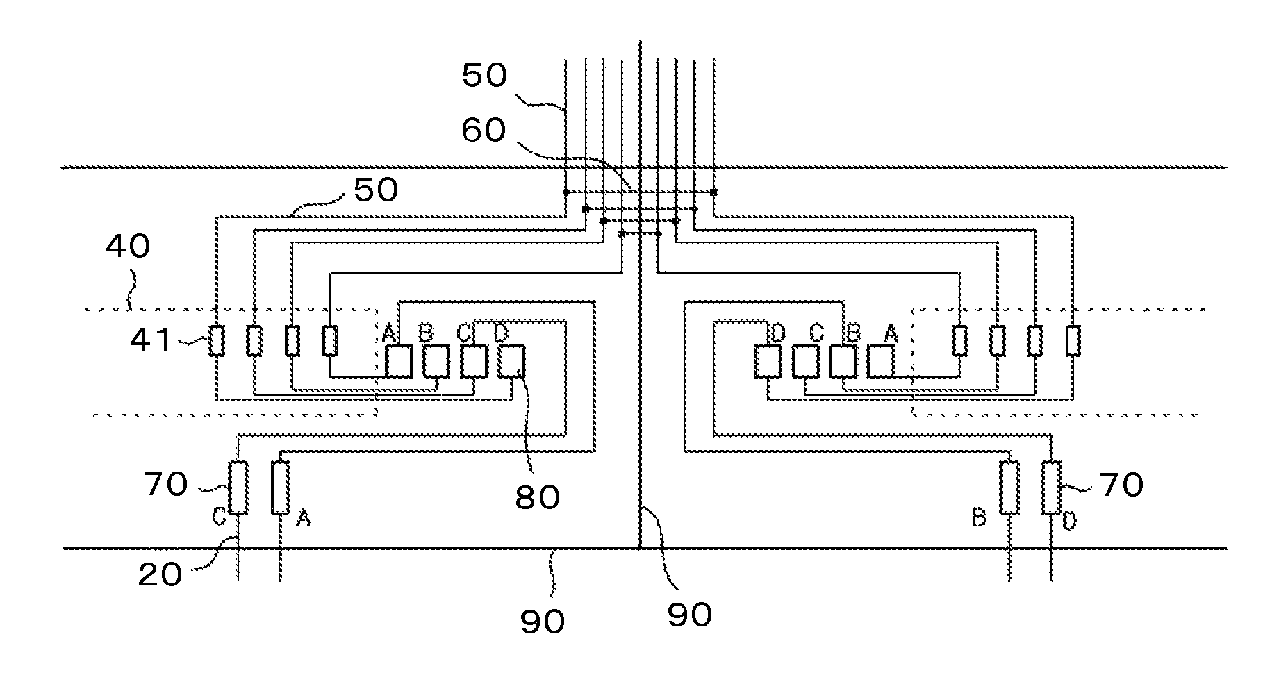
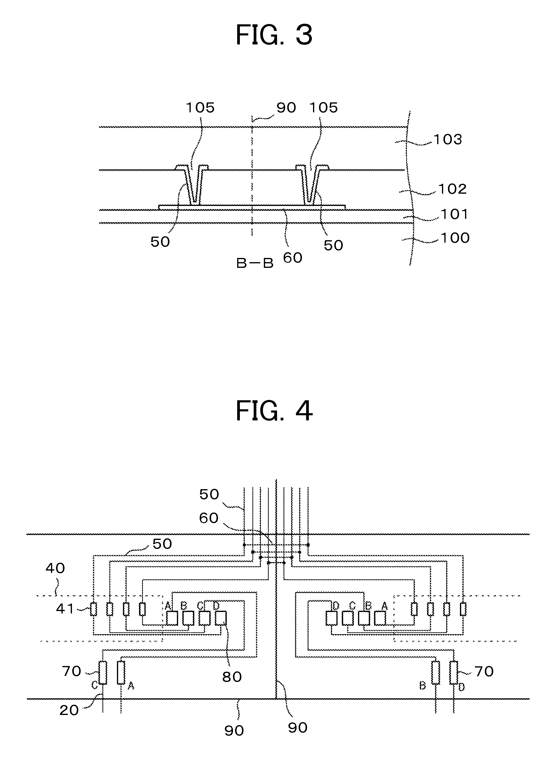
[0024]According to the present invention, there is provided a structure in which static electricity countermeasure wires are connected via flexible wiring substrate terminals to static electricity countermeasure elements formed outside liquid crystal cells. In this structure, the static electricity countermeasure wires of the adjacent liquid crystal cells on a mother TFT board are made common. This makes it possible to reduce the number of flexible wiring substrate terminals even as the number of signal lines increases in conjunction with the ever-higher resolution of the screen. That in turn can suppress the growing size of the liquid crystal cells resulting from the increasing number of the terminals.
[0025]Also, with the terminal count reduced, it is possible to prevent the flexible wiring substrate from growing in size. Furthermore, because the static electricity countermeasure wires can be connected to the static electricity countermeasure elements outside the liquid crystal cells under the same conditions, the liquid crystal cells having stable reliability can be manufactured.

Problems solved by technology

Because it is not efficient to manufacture individual liquid crystal display panels making up the liquid crystal display device, numerous liquid crystal cells are formed on a mother substrate that is later divided into individual liquid crystal cells.
Static electricity, if incurred during the manufacturing process, can lead to dielectric breakdown between wires or breakdown of TFTs.

Method used


Image

  • Liquid crystal display device preventing destruction by electro static charge
  • Liquid crystal display device preventing destruction by electro static charge
  • Liquid crystal display device preventing destruction by electro static charge

Examples


first embodiment

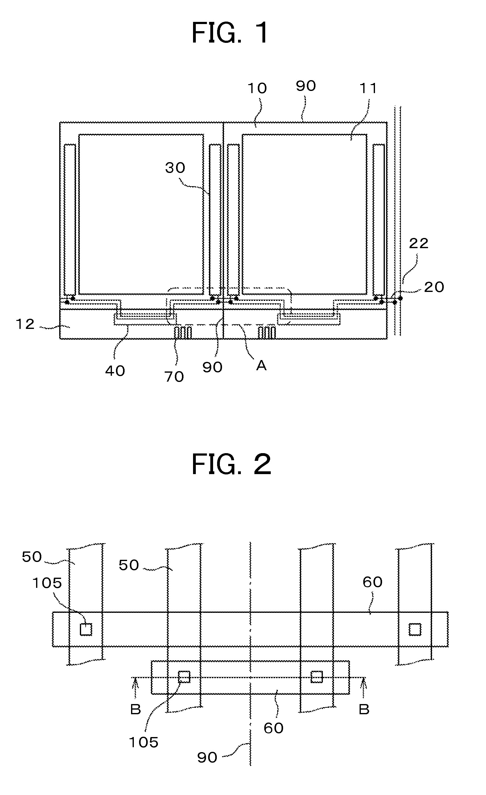
[0038]FIG. 1 is a plan view showing two TFT substrates according to the present invention, the substrates being located on a mother TFT substrate. On the TFT substrate shown in FIG. 1, built-in gate circuits 30 are formed on both sides of a display area 11. In FIG. 1, an IC driver amounting area 40 is formed in a terminal area 12. Some of the wires from the gate circuits 30 extend to the IC driver mounting area 40. Flexible wiring substrate terminals 70 are formed at the edge of the terminal area 12. In an ordinary setup, static electricity countermeasure wires 20 extend from the flexible wiring substrate terminals 70 to the outside.

[0039]In FIG. 1, the gate circuits 30 of the adjacent liquid crystal display panels are formed in a manner flanking a scribe line 60 that separates the liquid crystal cells from one another. To prevent dielectric breakdown caused by static electricity during the manufacturing process, the wires from the gate circuits 30 need to be connected via the stati...

second embodiment

[0049]FIG. 5 illustrates examples of the signal lines 50, connecting wires 60, flexible wiring substrate terminals 70, and static electricity countermeasure wires 20 making up the second embodiment. Also in FIG. 5, four wires from the gate circuit, not shown, in each liquid crystal cell are extended to the IC driver terminals 41 in the IC driver mounting area 40. The second embodiment is different from the first embodiment in FIG. 4 in that there are three flexible wiring substrate terminals 70 in the left-hand liquid crystal cell while there is one flexible wiring substrate terminal 70 in the right-hand liquid crystal cell.

[0050]In FIG. 5, the wires leading up to the inspection terminals 80 are the same as those in the first embodiment of FIG. 4. The difference is that the wires from the inspection terminals 80 up to the flexible wiring substrate terminals 70 are made different between the left-hand and the right-hand liquid crystal cells. This entails there being different numbers...

third embodiment

[0052]FIG. 6 illustrates examples of the signal lines 50, connecting wires 60, flexible wiring substrate terminals 70, and static electricity countermeasure wires 20 making up the third embodiment. Also in FIG. 6, four wires from the gate circuit, not shown, in each liquid crystal cell are extended to the IC driver terminals 41 in the IC driver mounting area 40. The difference between the third embodiment and the first embodiment in FIG. 4 is that the signal lines 50 in the left-hand liquid crystal cell are directly connected to the inspection terminals 80 without the intervention of the IC driver terminals 41 in the IC driver mounting area 40. The signal lines 50 in the right-hand liquid crystal cell are connected, as in the first embodiment of FIG. 4, to the IC driver terminals 41 in the IC driver mounting area 40 before being connected to the inspection terminals 80.

[0053]In the structure shown in FIG. 6 where the connections with the wires and terminals leading up to the flexibl...


PUM

PropertyMeasurementUnit
flexibleaaaaaaaaaa
semiconductoraaaaaaaaaa
light transmission rateaaaaaaaaaa

Abstract

This invention envisages having flexible wiring substrate terminals serving to connect with the wires for preventing dielectric breakdown caused by static electricity during the manufacturing process, and reducing the number of the flexible wiring substrate terminals. On a mother TFT substrate, signal lines extend over each liquid crystal cell in a manner flanking a scribe line between the adjacent liquid crystal cells. The signal lines of each liquid crystal cell are connected with connecting lines striding the scribe line. This reduces the number of static electricity countermeasure wires extending from the flexible wiring substrate terminals of each liquid crystal cell. Once completed, the individual liquid crystal cells are separated from one another, with no adverse effects caused by the connecting lines.

Description

CLAIM OF PRIORITY[0001]The present application claims priority from Japanese Patent Application JP 2013-183795 filed on Sep. 5, 2013, the content of which is hereby incorporated by reference into this application.BACKGROUND OF THE INVENTION[0002]1. Field of the Invention[0003]The present invention relates to a display device. More particularly, the invention relates to a liquid crystal display device in whose manufacturing process the destruction of wiring and other parts by static electricity is effectively prevented.[0004]2. Description of the Related Art[0005]In the liquid crystal display device, a TFT substrate having pixel electrodes and thin film transistors (TFTs) formed in a matrix thereon is opposed to a counter substrate having color filters or overcoat films formed at the locations corresponding to the pixel electrodes of the TFT substrate, the TFT substrate and the counter substrate sandwiching a liquid crystal therebetween. The light transmission rate of liquid crystal ...

Claims


Application Information

Patent Timeline
Patent Type & Authority Patents(United States)
IPC IPC(8): G02F1/1333G02F1/1343G02F1/1362G02F1/1345
CPCG02F1/136204G02F1/13458G02F1/133351
Inventor NISHINO, TOMONORIYANAGISAWA, SYOUAGATA, KENTAROABE, HIROYUKISUZUKI, TAKAYUKI
Owner JAPAN DISPLAY INC
Learn More