Partially-sprayed layer organic solar photovoltaic cell using a self-assembled monolayer and method of manufacture
a solar photovoltaic cell, self-assembled technology, applied in the direction of solid-state device manufacturing, sustainable manufacturing/processing, final product manufacturing, etc., can solve the problems of limiting the use of photovoltaic cells, complicated photovoltaic cell production processes, and increased energy consumption, etc., to achieve high temperature, low rate, and high manufacturing cost
- Summary
- Abstract
- Description
- Claims
- Application Information
AI Technical Summary
Benefits of technology
Problems solved by technology
Method used
Image
Examples
example
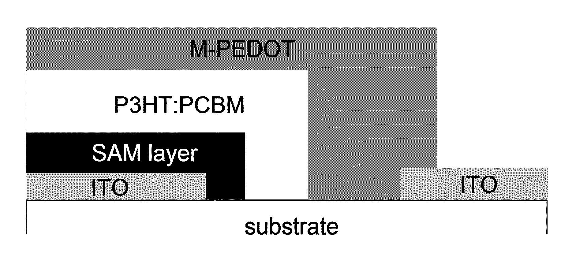
[0029]The indium tin oxide (ITO) is patterned onto a glass substrate using a positive photo resist, such as Shipley 1813, spin coated at 4500 rpm and soft baked on a hotplate for 3 minutes at 90° C. The substrate is then exposed to a UV-lamp for 1.4 seconds in a constant intensity mode set to 25 watts. The structure was developed for about 2.5 minutes using Shipley MF319 and rinsed with water. The substrate was then hard-baked, at 145° C. for 4 minutes and any excess photoresist cleaned off with acetone and cotton. After cleaning, the substrate was etched from about 5-11 minutes with a solution of 20% HCl-7% HNO3 on a hotplate at 100° C. The etched substrate was then cleaned by hand using acetone followed by isopropanol and UV-ozone cleaned for at least 15 minutes.
[0030]The Self-Assembled Monolayer (SAM) layer was formed on top of the patterned ITO layer. A solution of N-propyl trimethoxysilane (3 mM) in ethanol was prepared and stirred for 10 minutes at room temperature. Once the S...
example 2
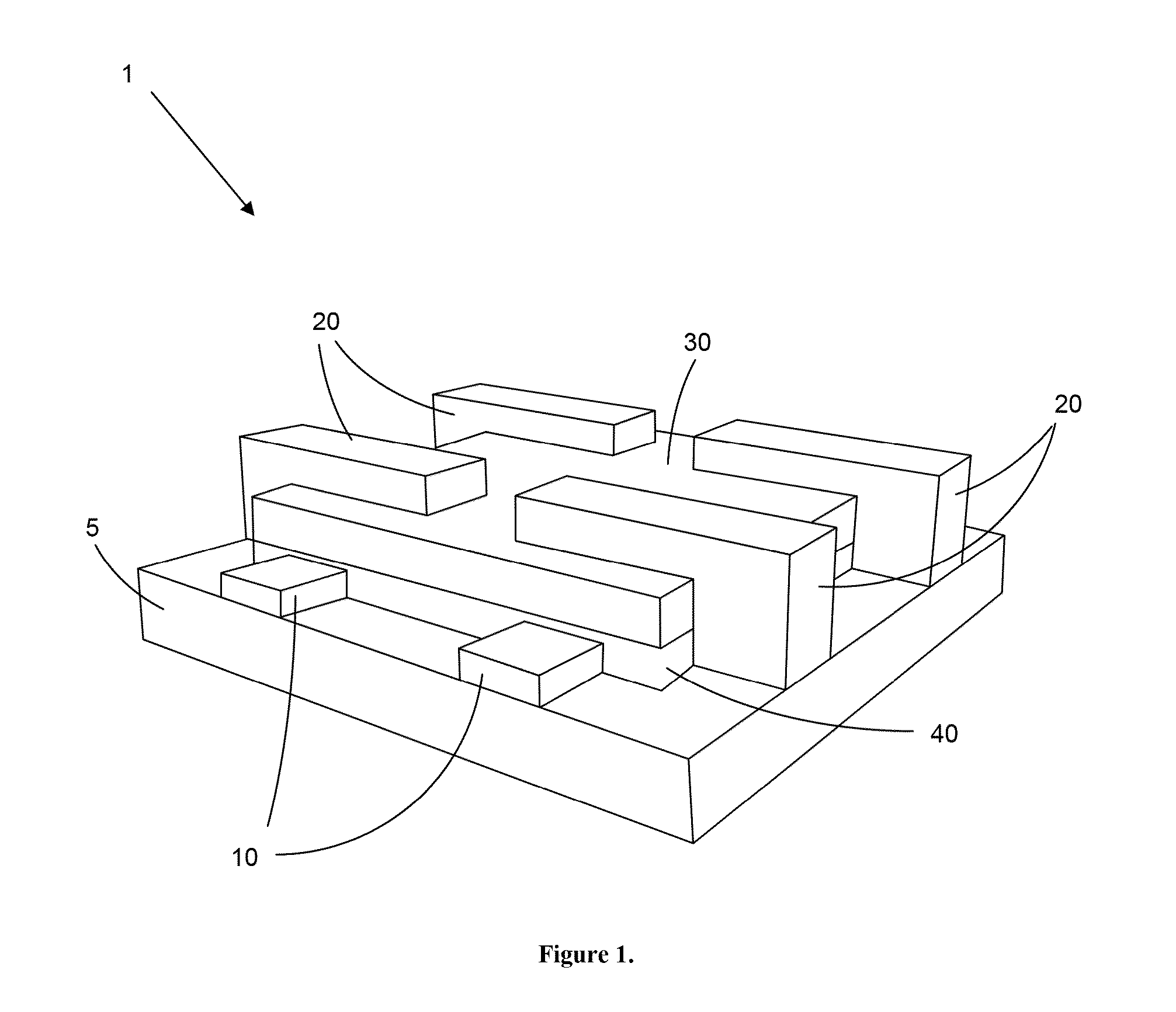
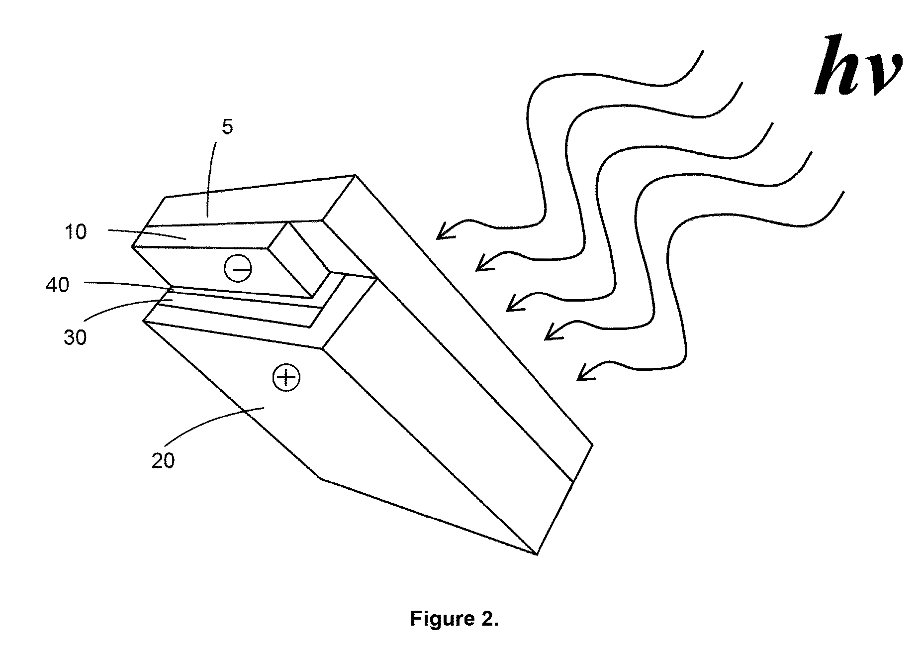
[0036]Inverted organic photovoltaic cell 1, seen dissected in FIG. 1, was created using the method described in Example 1. Inverted photovoltaic cell 1 was composed of different layers of active materials and terminals (anode and cathode) built onto substrate 5. Anode 10, comprised of ITO in the present example, was sprayed onto substrate 5 forming a ‘’ pattern extending from a first set of edges of substrate 5. SAM layer 40 covers anode 10, except for the outermost edges, as seen in FIG. 2. The components of the SAM layer were chosen to provide a gradient for charges crossing the interface, approximating a conventional p-n junction with organic semiconductors, thereby providing an increased efficiency of heterojunctions. Active layer 30 is disposed directly on top of interfacial buffer layer 40, and was prepared using poly(3-hexylthiophene) and 6,6-phenyl C61 butyric acid methyl ester. Anode 20 was disposed on the active layer in a pattern, similar to the cathode, but perpendicular...
example 3
[0038]Solar illumination has been demonstrated to improve solar array efficiency up to 250%. Device efficiency of 1.80% was observed with the array under AM1.5 irradiance. Data have shown that the performance enhancement under illumination only happens with sprayed devices, not devices made by spin coating (See, Lewis, et al., PCT / US11 / 54290). This means that solar cells made using the present spray-on technique perform better under sunlight, which is beneficial for solar energy application.
[0039]A solar array was prepared by forming 50 individual inverted cells as described above, each with an active area of 60 mm2. The array was configured with 10 cells in series in one row to increase the voltage, and five rows in parallel connection to increase the current. The neighboring cells were connected using the organic layer configuration, seen in FIG. 4 and in cross section in FIG. 5.
[0040]In the preceding specification, all documents, acts, or information disclosed does not constitute...
PUM
| Property | Measurement | Unit |
|---|---|---|
| thickness | aaaaa | aaaaa |
| thickness | aaaaa | aaaaa |
| thickness | aaaaa | aaaaa |
Abstract
Description
Claims
Application Information
 - R&D
- Intellectual Property
- Life Sciences
- Materials
- Tech Scout
- Unparalleled Data Quality
- Higher Quality Content
- 60% Fewer Hallucinations
Browse by: Latest US Patents, China's latest patents, Technical Efficacy Thesaurus, Application Domain, Technology Topic, Popular Technical Reports.
© 2025 PatSnap. All rights reserved.Legal|Privacy policy|Modern Slavery Act Transparency Statement|Sitemap|About US| Contact US: help@patsnap.com


