Liquid crystal display device

a liquid crystal display and display screen technology, applied in non-linear optics, instruments, optics, etc., can solve the problems of insufficient storage capacitance, inability to increase the aperture ratio, and inability to widen the range of driving liquid crystal molecules in the sub-pixel, so as to achieve sufficient storage capacitance. the effect of sufficient assuran

Active Publication Date: 2016-07-12
TIANMA MICRO ELECTRONICS CO LTD +1
View PDF8 Cites 0 Cited by
  • Summary
  • Abstract
  • Description
  • Claims
  • Application Information

AI Technical Summary

Benefits of technology

[0011]According to the present invention, when viewed from a direction perpendicular to the substrate, the pixel electrode or the common electrode can be disposed closer to the data line side, and while generating an electric field for driving liquid crystal molecules more widely in the sub pixel, the storage capacitance can be sufficiently assured.

Problems solved by technology

The electrode has to be disposed apart from the data line for the clearance, the range of driving the liquid crystal molecules cannot be widened in the sub pixel, and it causes a problem that the aperture ratio cannot be increased.
For example, in the liquid crystal display device, the data line and the pixel electrode are in the same layer, so that the connecting part of the pixel electrode has to be disposed apart from the data line, and there is a problem such that the range of driving the liquid crystal molecules cannot be widened in the sub pixel.
Since the storage capacitance is generated on the short side of a pixel in structure, large area cannot be assured, and there is a problem such that sufficient storage capacitance cannot be assured.

Method used


Image

  • Liquid crystal display device
  • Liquid crystal display device
  • Liquid crystal display device

Examples


first embodiment

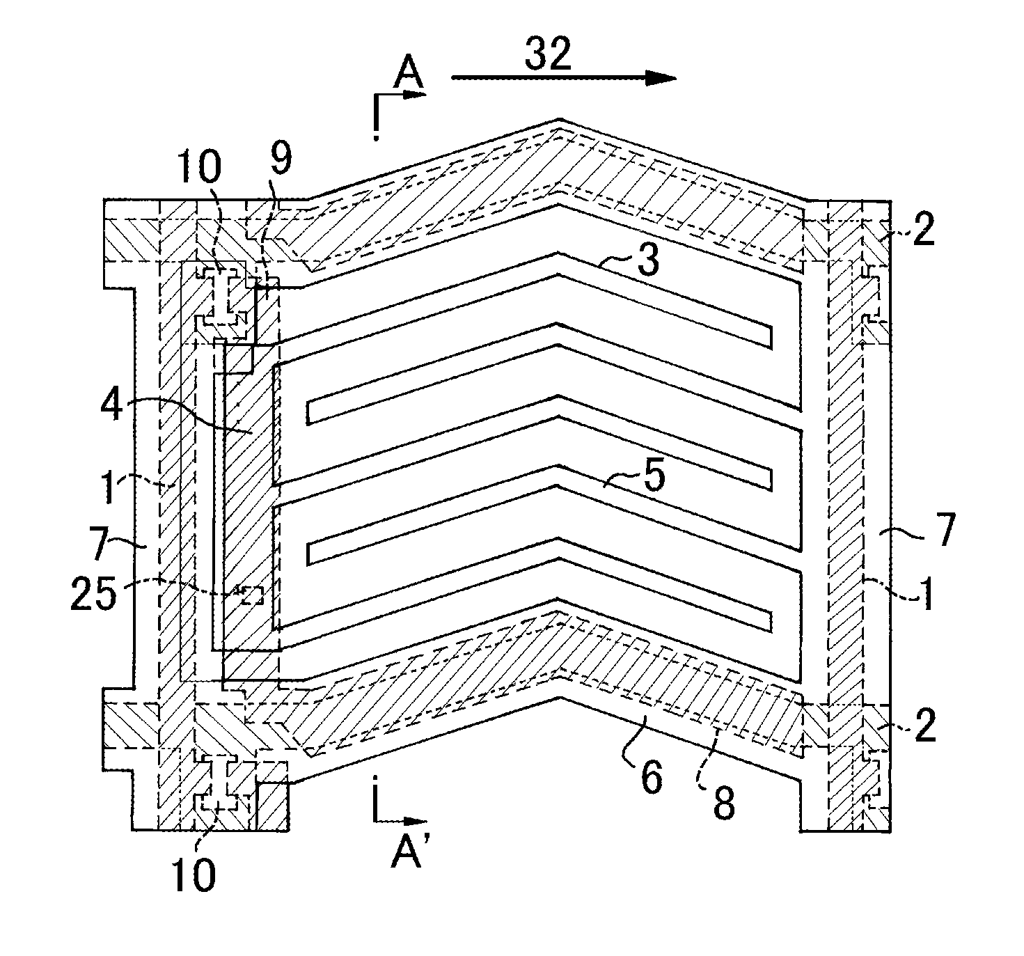
[0023]As illustrated in FIG. 1, in a liquid crystal display device, a plurality of data lines 1 are disposed in parallel to one another on a transparent substrate (first substrate). A plurality of scan lines 2 are disposed substantially perpendicular to the data lines 1. By the plurality of data lines 1 and the scan lines 2, a plurality of sub pixel regions arranged in a matrix are defined.

[0024]A gate electrode is provided on the scan line 2 near a part crossing the data line 1, and the drain electrode is connected from the data line 1 crossing the scan line 2. With such a structure, a thin film transistor can be formed near the crossing part of the data line 1 and the scan line 2.

[0025]On one of the sides of the data line 1, a source pixel electrode (an electric potential supply line connected to the source electrode) is disposed along the data line 1, and the source electrode of the TFT is connected to the source pixel electrode

[0026]Pixel electrodes are disposed in a layer upper...

second embodiment

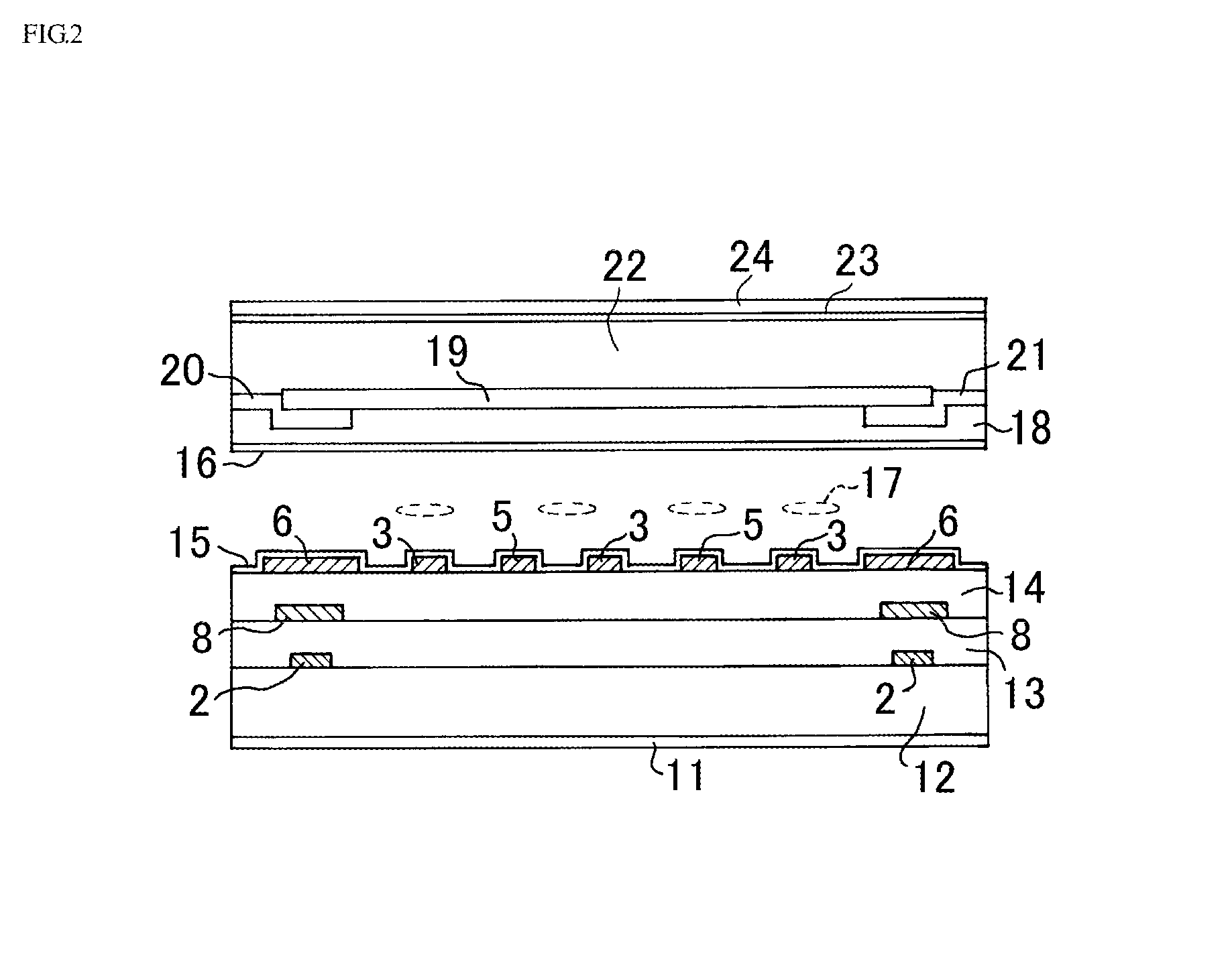
[0057]A second embodiment of the present invention will be described with reference to FIGS. 5 and 6. FIG. 5 is a plan view illustrating the configuration of one sub pixel in a liquid crystal display device as a second embodiment of the present invention. FIG. 6 is a cross section taken along line A-A′ of FIG. 5.

[0058]The pixel of the second embodiment illustrated in FIGS. 5 and 6 will be described in detail in fabricating order.

[0059]First, on a glass substrate as the first insulating substrate 12, the scan line 2 is formed by a first metal layer made by 2500 A of Cr.

[0060]As the gate insulating film 13, 5000 A of SiNx and a thin film semiconductor layer made of 2000 A of a-Si and 500 A of n-a-Si are formed. The thin film semiconductor layer 10 is patterned while leaving only a TFT part provided as a switching element of the pixel. By a second metal layer made by 2500 A of Cr, the data line 1, source / drain electrodes of the TFT, the source pixel electrode 9 connected to the source ...

third embodiment

[0083]A third embodiment of the present invention will be described with reference to FIGS. 7, 8, and 9. FIG. 7 is a plan view illustrating the configuration of one sub pixel in a liquid crystal display device as a third embodiment of the present invention. FIG. 8 is a cross section of a TFT substrate, taken along line A-A′ in FIG. 7.

[0084]The pixel of the second embodiment illustrated in FIGS. 7 to 9 will be described in detail in fabricating order.

[0085]First, on a glass substrate as the first insulating substrate 12, the scan line 2 is formed by a first metal layer made by 2500 A of Cr.

[0086]As the gate insulating film 13, 5000 A of SiNx and a thin film semiconductor layer made of 2000 A of a-Si and 500 A of n-a-Si are formed. The thin film semiconductor layer 10 is patterned while leaving only a TFT part provided as a switching element of the pixel. By a second metal layer made by 2500 A of Cr, the data line 1, source / drain electrodes of the TFT, the source pixel electrode 9 con...


PUM

PropertyMeasurementUnit
θaaaaaaaaaa
widthaaaaaaaaaa
θaaaaaaaaaa

Abstract

A transverse electric field-type liquid crystal display device displays by rotating homogeneous-aligned liquid crystals by a transverse electric field substantially parallel to a substrate, applied across a pixel electrode and a common electrode, assuring sufficient storage capacitance while enlarging the area of driving the liquid crystal molecules in a sub pixel. A source pixel electrode connected to a source electrode extends along the data line, a storage capacitance electrode formed by the same layer as the data line is formed above an adjacent scan line so as to overlap the adjacent scan line, the source pixel electrode is disposed so as to be connected to the storage capacitance electrode and a pixel along one side, an interlayer film is formed over the source pixel electrode, and a pixel electrode and a common electrode formed by a transparent conductive film are formed over the interlayer film.

Description

TECHNICAL FIELD[0001]The present invention relates to a liquid crystal display device and, more particularly, to an active-matrix-type liquid crystal display device in which liquid crystal molecules are driven with an electric field substantially perpendicular to a thin film transistor substrate.BACKGROUND ART[0002]A liquid crystal display device of a TN (Twisted Nematic) type being widely used has high contrast but, on the other hand, has a problem of high visual angle dependence since the molecular axis of the liquid crystal rises due to the vertical electric field. Since demand for a large-sized monitor of a TV or the like is increasing in recent years, a so-called transverse-electric-field-type liquid crystal panel such as the IPS (In-Plane Switching) type or FFS type is being spread, in which an electric field substantially parallel to a substrate for which thin film transistors (hereinafter, called TFTs) are provided is applied to liquid crystal molecules to drive the molecule...

Claims


Application Information

Patent Timeline
Patent Type & Authority Patents(United States)
IPC IPC(8): G02F1/1343G02F1/1362G02F1/1337
CPCG02F1/133753G02F1/134363G02F1/136213G02F1/133345G02F1/133512G02F1/133514G02F1/133516G02F1/133528G02F1/133784G02F1/13394G02F1/1341G02F1/134336G02F1/13439G02F1/136286G02F1/1368G02F1/133302G02F1/133519G02F1/133531G02F1/134345
Inventor NISHIDA, SHINICHITAGUCHI, NAOYUKIWATANABE, TAKAHIKO
Owner TIANMA MICRO ELECTRONICS CO LTD
Why Eureka
Try Eureka