Eureka AIR delivers breakthrough ideas for toughest innovation challenges, trusted by R&D personnel around the world.

Laser induced thermal imaging device and laser induced thermal imaging method

a thermal imaging and laser induced technology, applied in lasers, solid-state devices, printing, etc., can solve problems such as difficulty in confirming position inferiority, and achieve the effect of preventing or reducing position inferiority (or error or misalignment) of imaging patterns and reliable pattern precision

Active Publication Date: 2016-05-10
SAMSUNG DISPLAY CO LTD
View PDF13 Cites 0 Cited by
  • Summary
  • Abstract
  • Description
  • Claims
  • Application Information

AI Technical Summary

Benefits of technology

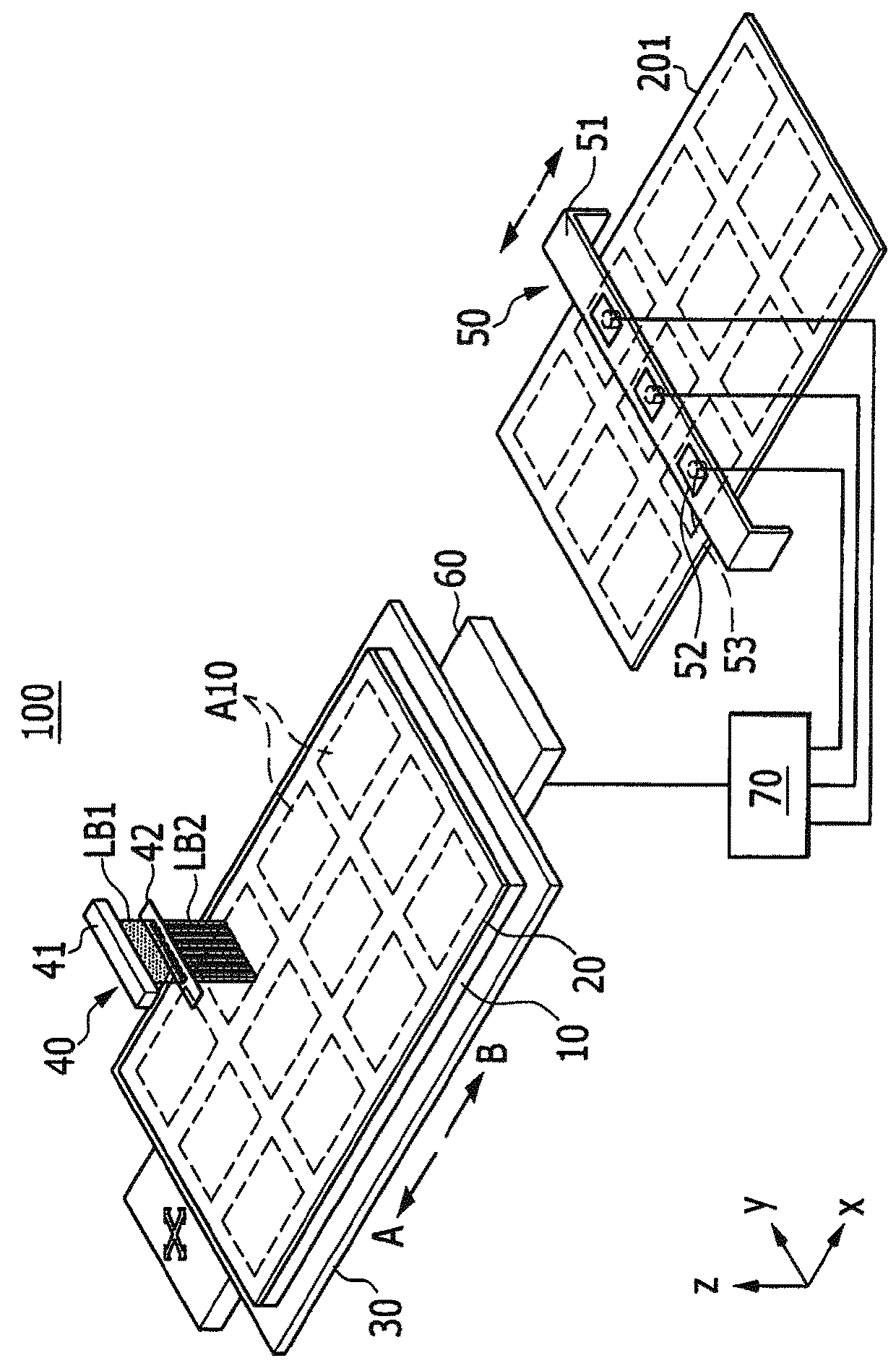
[0010]Embodiments of the present invention have been made in an effort to provide a laser induced thermal imaging device and a laser induced thermal imaging method, in which a position of a laser beam and a position of a pixel region can be automatically precisely compensated for every substrate during an imaging process to prevent or reduce position inferiority (or error or misalignment) of an imaging pattern and ensure a reliable pattern precision.
[0020]According to exemplary embodiments of the present invention, a feedback of a pattern error measured by an error measurement portion can be provided to a stage moving portion to automatically correct the pattern error. Accordingly, it is possible to automatically and precisely correct positions of pixel regions for every substrate during a thermal imaging process, thereby preventing or reducing position inferiority (or error or misalignment) of an imaging pattern, and ensuring a reliable pattern precision.

Problems solved by technology

However, when using the aforementioned method, there is a technical limitation in that it is difficult to confirm position inferiority (e.g., error or misalignment) of an imaging pattern during an imaging process in mass-production before the position of the laser beam and the position of the pixel region are confirmed from the waste donor film.

Method used


Image

  • Laser induced thermal imaging device and laser induced thermal imaging method
  • Laser induced thermal imaging device and laser induced thermal imaging method
  • Laser induced thermal imaging device and laser induced thermal imaging method

Examples


Embodiment Construction

[0029]The exemplary embodiment will be described more fully hereinafter with reference to the accompanying drawings, in which exemplary embodiments of the invention are shown. As those skilled in the art would realize, the described embodiments may be modified in various different ways, all without departing from the spirit or scope of the present invention.

[0030]In the specification, unless explicitly described to the contrary, the word “comprise” and variations such as “comprises” or “comprising”, will be understood to imply the further inclusion of other elements. Further, in the specification, it will be understood that when an element such as a layer, a film, a region, or a substrate is referred to as being “over” or “on” another element, it can be “directly on” the other element or intervening elements may also be present. Further, the word “over” or “on” means positioning on or below the object portion, but does not essentially mean positioning on the upper side of the object...


PUM

PropertyMeasurementUnit
distanceaaaaaaaaaa
displacementaaaaaaaaaa
induced thermal imagingaaaaaaaaaa

Abstract

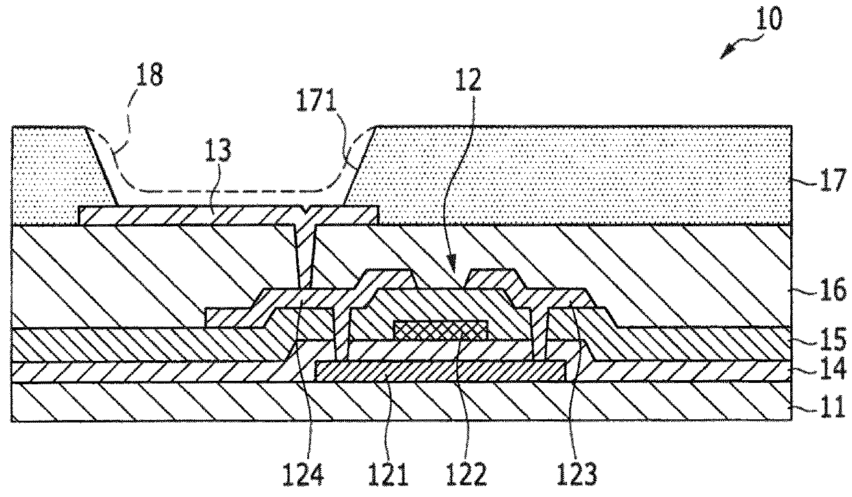
A laser induced thermal imaging device includes a substrate stage configured to support a substrate and a donor film; a beam radiation portion configured to emit a laser beam toward the donor film to image an imaging layer of the donor film on a pixel region on the substrate; an error measurement portion configured to determine a position of the laser beam and a position of the pixel region from the donor film to measure a pattern error; and a stage moving portion configured to move the substrate stage in accordance with the pattern error to correct the pattern error.

Description

CROSS-REFERENCE TO RELATED APPLICATION[0001]This application claims priority to and the benefit of Korean Patent Application No. 10-2013-0040652 filed in the Korean Intellectual Property Office on Apr. 12, 2013, the entire contents of which are incorporated herein by reference.BACKGROUND[0002]1. Field[0003]Aspects of embodiments of the present invention relate to a laser induced thermal imaging device and a laser induced thermal imaging method, and more particularly, to a laser induced thermal imaging device and a laser induced thermal imaging method, in which an organic emission layer is formed on a substrate by using a donor film.[0004]2. Description of the Related Art[0005]Recently, a laser induced thermal imaging method using a laser induced thermal imaging device has been used as a method of forming an organic emission layer of an organic light emitting diode display.[0006]The laser induced thermal imaging method is formed of a process of disposing a base film and a donor film ...

Claims


Application Information

Patent Timeline
Patent Type & Authority Patents(United States)
IPC IPC(8): H01L51/00
CPCH01L51/0013H01L51/0031H10K71/18H10K71/70B41J2/455B41M5/00H01S3/00H10K71/00
Inventor JEUN, JIN-HONGLEE, YUNA
Owner SAMSUNG DISPLAY CO LTD
Why Eureka
Eureka Blog
Learn More