
Holographic waveguide display

a waveguide display and waveguide technology, applied in the direction of viewfinders, planar/plate-like light guides, instruments, etc., can solve the problems of cumbersome form factors, insufficient, and current wearable displays only manage to deliver see through, so as to minimize laser speckle

Active Publication Date: 2016-05-10
DIGILENS
View PDF9 Cites 75 Cited by
  • Summary
  • Abstract
  • Description
  • Claims
  • Application Information

AI Technical Summary

Benefits of technology

The solution enables a compact, transparent, and high-contrast information display that is easily wearable, with adjustable diffraction efficiency and minimal disturbance to ambient light, enhancing visibility and image quality even in demanding conditions.

Problems solved by technology

The above goals are not achieved by current technology.
Current wearable displays only manage to deliver see through, adequate pupils, eye relief and field of view and high brightness simultaneously at the expense of cumbersome form factors.
In many cases weight is distributed in the worst possible place for a wearable display, in front of the eye.
Microdisplays, which provide high-resolution image generators in tiny flat panels, do not necessarily help with miniaturizing wearable displays because the requirement for very high magnifications inevitably results in large diameter optics.
Several ultra low form factor designs offering spectacle-like form factors are currently available but usually require aggressive trade-offs against field of view, eye relief and exit pupil.
A Bragg grating is then recorded by illuminating the liquid material with two mutually coherent laser beams, which interfere to form the desired grating structure.
When an electric field is applied to the hologram via the electrodes, the natural orientation of the LC droplets is changed thus reducing the refractive index modulation of the fringes and causing the hologram diffraction efficiency to drop to very low levels.

Method used


Image

  • Holographic waveguide display
  • Holographic waveguide display
  • Holographic waveguide display

Examples


Embodiment Construction

[0059]The invention will now be further described by way of example only with reference to the accompanying drawings.

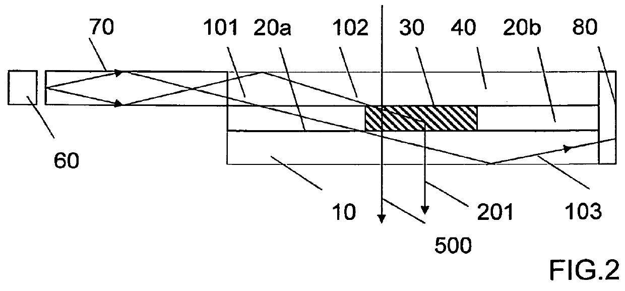
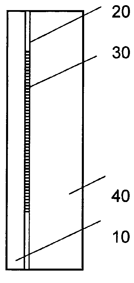
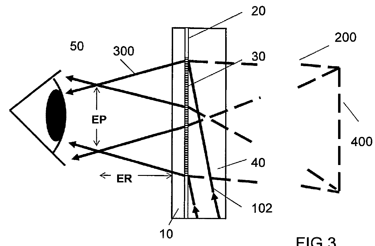
[0060]FIG. 1 shows a schematic side elevation view of a portion of one eyepiece of a wearable display in one embodiment of the invention. Although a planar element is shown the complete eyepiece may have a curved or facetted surface. The portion of the display shown in FIG. 1 comprises a DOE 10 an HPDLC layer comprising flood cured region indicated by 20 surrounding at least one independently switchable SBG region indicated by 30 and a transparent substrate layer 40. The HPDLC layer is sandwiched between the substrate and the DOE. Said SBG regions may be information symbols. Alternatively, the SBG regions may be configured to provide two dimensional pixelated arrays. In each case the SBGs are confined to the symbol or pixel regions the display being perfectly transparent elsewhere. The SBG and DOE together encode the characteristics of a lens whose function will be ex...


PUM

PropertyMeasurementUnit
Bragg angleaaaaaaaaaa
refractive indexaaaaaaaaaa
thicknessesaaaaaaaaaa

Abstract

A holographic waveguide display comprises: a source of light; at least one switchable grating layer comprising a multiplicity of grating regions each switchable between a diffracting state and a non diffracting state; means for spatio-temporally modulating light from the source to provide image light comprising at least one beam deflector for scanning the light in at least one of two orthogonal directions and at least one modulator for amplitude modulating the light. A first scanned angular range of light is diffracted through a first area into a first field of view by a first set of grating regions, and through a second area into to the first field of view by a second set of grating regions. Each grating region of the first and second sets has a first grating function. The first and second areas lie within an exit pupil of the display.

Description

REFERENCE TO EARLIER FILINGS[0001]The present patent application is a continuation of a U.S. patent application Ser. No. 13 / 317,468 filed on Oct. 19, 2011, which is the national phase application of PCT application No.: PCT / GB2010 / 000835 filed 27 Apr. 2010, entitled COMPACT HOLOGRAPHIC EDGE ILLUMINATED WEARABLE DISPLAY, claiming priority to U.S. provisional patent application 61 / 202,996 filed on 27 Apr. 2010, entitled COMPACT HOLOGRAPHIC EDGE ILLUMINATED EYEGLASS DISPLAY.[0002]This application incorporates by reference in their entireties: PCT Application No.: US2008 / 001909, with International Filing Date: 22 Jul. 2008, entitled LASER ILLUMINATION DEVICE; U.S. patent application Ser. No. 10 / 555,661 filed 4 Nov. 2005 entitled SWITCHABLE VIEWFINDER DISPLAY; and PCT Application No. US2006 / 043938 with International Filing Date: 13 Nov. 2006, entitled METHOD AND APPARATUS FOR PROVIDING A TRANSPARENT DISPLAY.BACKGROUND OF THE INVENTION[0003]This invention relates to a wearable display dev...

Claims


Application Information

Patent Timeline
Patent Type & Authority Patents(United States)
IPC IPC(8): G02B6/34G02B26/10G02F1/29G02F1/1334G02B27/48G03B13/02F21V8/00G02B27/01G02B26/08G03H1/22
CPCG02F1/292G02B6/0011G02B26/101G02B26/105G02B27/0172G02B27/48G02F1/13342G03B13/02G02B26/0808G02B2027/0107G02B2027/0174G02B2027/0194G02F2201/307G03H2001/2226G03B21/10G02B5/1828G02B5/1876G02B6/34
Inventor POPOVICH, MILAN MOMCILOWALDERN, JONATHAN DAVID
Owner DIGILENS
Learn More