Spark plug
a technology of spark plugs and electrodes, applied in spark plugs, machines/engines, mechanical equipment, etc., can solve the problems of deformation of parts of chips on the opposite side of the electrode, detachment of chips from the electrodes, and small thermal stress difference between electrodes and chips, so as to improve weldability and reduce the effect of thermal stress
- Summary
- Abstract
- Description
- Claims
- Application Information
AI Technical Summary
Benefits of technology
Problems solved by technology
Method used
Image
Examples
first embodiment
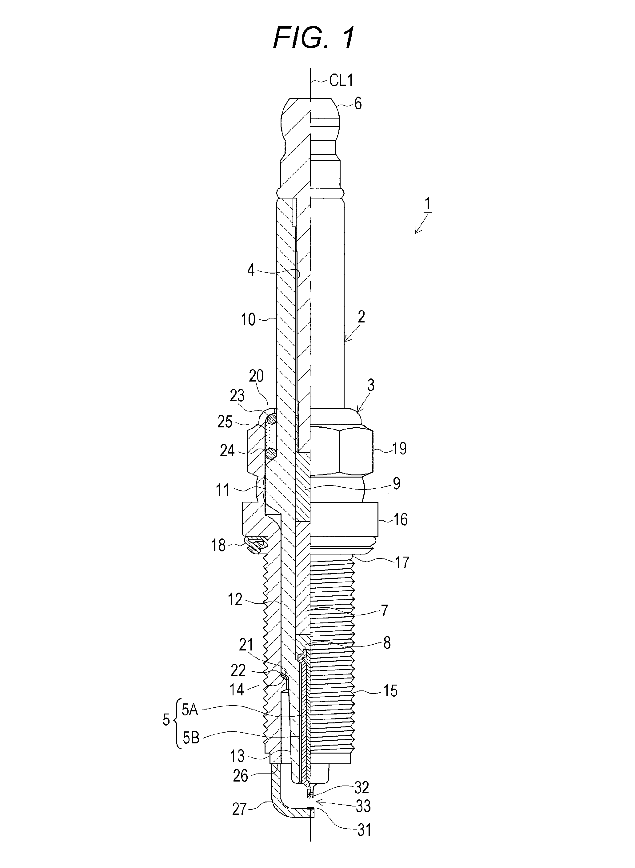
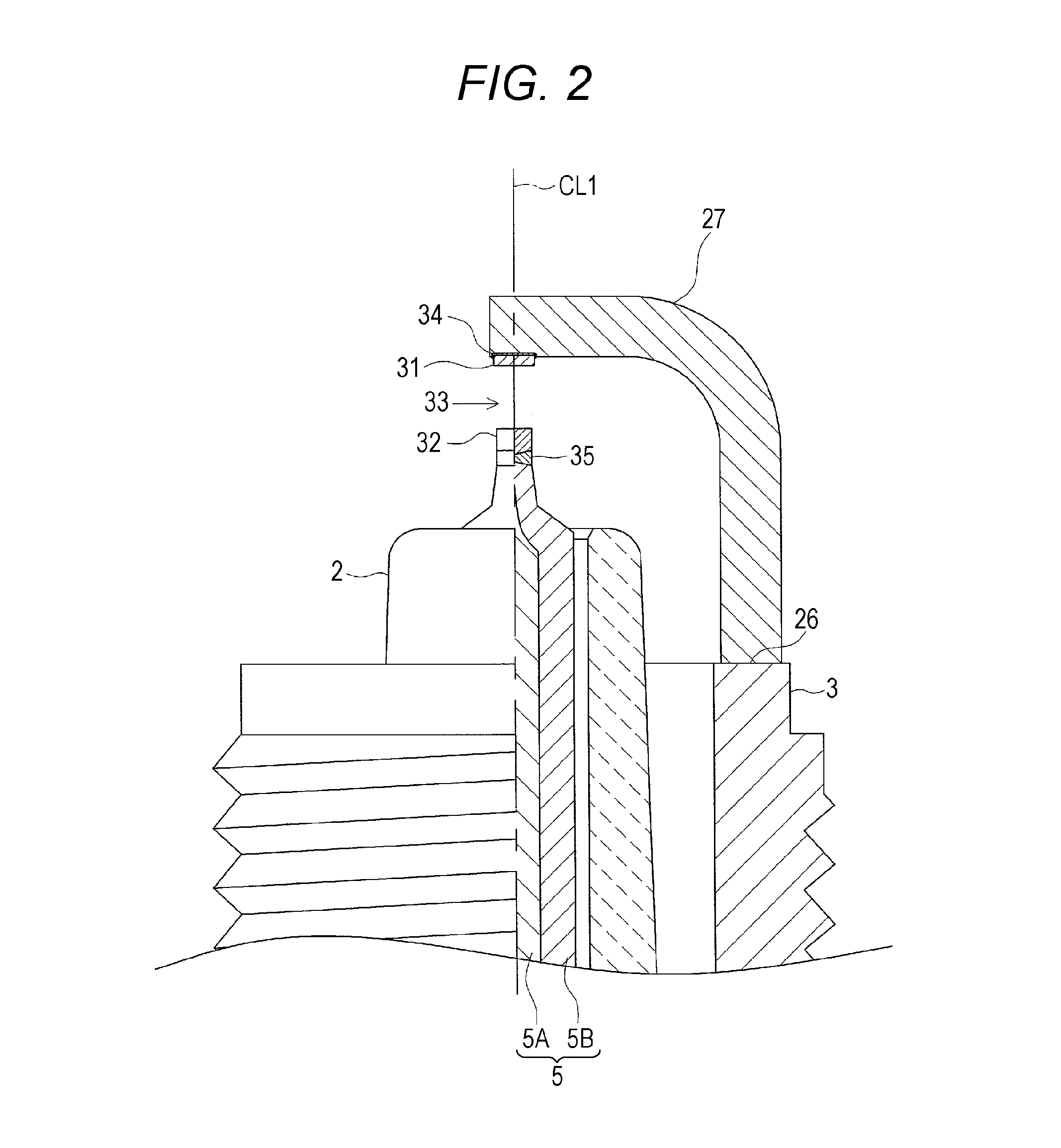
[0035]FIG. 1 is a partial sectional front view of a spark plug 1. In FIG. 1, the direction of an axial line CL1 of the spark plug 1 corresponds to the top-bottom direction in the drawing, with the bottom and top corresponding to the tip side and the rear end side of the spark plug 1, respectively.
[0036]The spark plug 1 includes such as a cylindrical ceramic insulator 2, and a cylindrical metal shell 3 holding the ceramic insulator 2.
[0037]The ceramic insulator 2 is formed by sintering alumina and the like in a well-known manner, and includes, in terms of its outer shape, a rear end-side body portion 10 formed on the rear end side, an large-diameter portion 11 located closer to the tip side than the rear end-side body portion 10 and projecting radially outwardly, a middle body portion 12 located closer to the tip side than the large-diameter portion 11 with a smaller diameter than the diameter of the large-diameter portion 11, and an insulator nose portion 13 located closer to the ti...
second embodiment
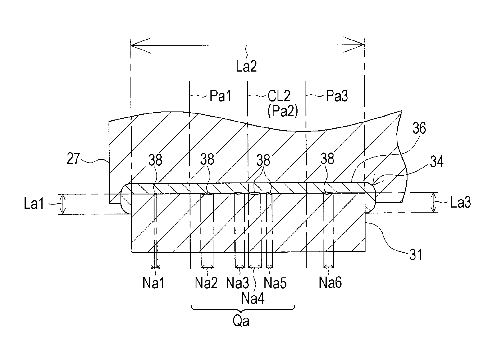
[0067]In the following, a second embodiment will be described while focusing on differences from the first embodiment. According to the first embodiment, the intermediate layer 34 is formed over the entire area between the ground electrode-side chip 31 and the ground electrode 27, and the intermediate layer 35 is formed over the entire area between the center electrode-side chip 32 and the center electrode 5 (outer layer 5B). In contrast, according to the second embodiment, by varying the weld conditions, an intermediate layer 44 is formed in a part of the area between the ground electrode-side chip 41 and the ground electrode 27, as illustrated in FIG. 9, and an intermediate layer 45 is formed in a part of the area between the center electrode-side chip 42 and the center electrode 5 (outer layer 5B). According to the present embodiment, as illustrated in FIG. 10, in order to ensure sufficient weldability of the ground electrode-side chip 41 with respect to the ground electrode 27, ...
third embodiment
[0076]A third embodiment will be described while focusing on differences from the first and the second embodiments. In the first and the second embodiments, the ground electrode-side chips 31 and 41 are entirely positioned on the proximal side with respect to the tip of the ground electrode 27. In contrast, according to the third embodiment, as illustrated in FIG. 14, a ground electrode-side chip 51 is welded to the ground electrode 27 with a part of the ground electrode-side chip 51 projecting beyond the tip of the ground electrode 27. In order to ensure sufficient weldability of the ground electrode-side chip 51 with respect to the ground electrode 27, the length of the boundary of the ground electrode-side chip 51 and the intermediate layer 54 is made greater than the length of a part of the ground electrode-side chip 51 that adjoins the ground electrode 27 without the intermediate layer 54.
[0077]In addition, the ground electrode-side chip 51 is cuboidal as in the second embodime...
PUM
 Abstract
Description
Claims
Application Information
 - R&D
- Intellectual Property
- Life Sciences
- Materials
- Tech Scout
- Unparalleled Data Quality
- Higher Quality Content
- 60% Fewer Hallucinations
Browse by: Latest US Patents, China's latest patents, Technical Efficacy Thesaurus, Application Domain, Technology Topic, Popular Technical Reports.
© 2025 PatSnap. All rights reserved.Legal|Privacy policy|Modern Slavery Act Transparency Statement|Sitemap|About US| Contact US: help@patsnap.com


