
Organic photovoltaic cell, organic semiconductor polymer and composition for organic semiconductor material used therefor

a technology of organic semiconductor and photovoltaic cells, which is applied in the direction of organic conductors, non-metal conductors, conductors, etc., can solve the problems of insufficient photoelectric conversion efficiency of organic photovoltaic cells, and achieve excellent inhibiting effect, reduce photoelectric conversion efficiency, and improve photoelectric conversion efficiency.

Active Publication Date: 2015-12-15
FUJIFILM CORP
View PDF4 Cites 0 Cited by
  • Summary
  • Abstract
  • Description
  • Claims
  • Application Information

AI Technical Summary

Benefits of technology

[0029]The organic photovoltaic cell of the present invention excels in both photoelectric conversion efficiency and durability (durability in the presence of oxygen in particular). Further, the organic photovoltaic cell of the present invention exerts an excellent inhibiting effect on a decrease in photoelectric conversion efficiency even in the case where the cell size is increased as needed. Furthermore, the polymer of the present invention and the composition containing the same are novel, and are useful as a semiconductor material used for the above-described solar cell and the like.
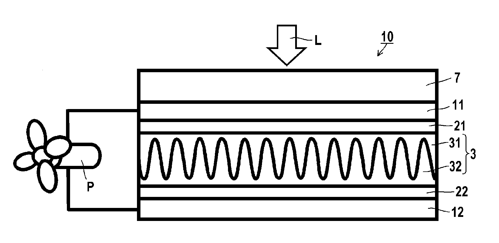
[0030]Other and further features and advantages of the invention will appear more fully from the following description, appropriately referring to the accompanying drawing.

Problems solved by technology

However, the photoelectric conversion efficiency of organic photovoltaic cells is still insufficient.

Method used


Image

  • Organic photovoltaic cell, organic semiconductor polymer and composition for organic semiconductor material used therefor
  • Organic photovoltaic cell, organic semiconductor polymer and composition for organic semiconductor material used therefor
  • Organic photovoltaic cell, organic semiconductor polymer and composition for organic semiconductor material used therefor

Examples


examples

[0179]The present invention will be described in more detail based on examples given below, but the invention is not meant to be limited by these.

synthesis example

Synthesis of Polymer 1

[0180]The homopolymer (Polymer 1) derived from Compound A as a monomer was synthesized with reference to the method described in Macromolecules, 1992, Vol. 25, pp. 1214 to 1223. Herein, the Compound A was synthesized referring to the method described in Chemische Berichte, 1991, Vol. 124, pp. 2481 to 2488.

[0181]

Synthesis of Polymer 2

[0182]The homopolymer (Polymer 2) derived from Compound B as a monomer was synthesized in the same manner as Polymer 1. Herein, the Compound B was synthesized referring to the method described in Japanese Patent No. 4414881.

[0183]

Synthesis of Polymer 3

[0184]The homopolymer (Polymer 3) derived from Compound C as a monomer was synthesized in the same manner as Polymer 1. Herein, the Compound C was synthesized referring to the method described in Journal of the Chemical Society, Perkin Transactions 1, 1994, Vol. 21, pp. 3065 to 3070.

[0185]

Synthesis of Polymer 4

[0186]The homopolymer (Polymer 4) derived from Compound D as a monomer was s...


PUM

PropertyMeasurementUnit
wavelengthaaaaaaaaaa
flow rateaaaaaaaaaa
flow rateaaaaaaaaaa

Abstract

An organic photovoltaic cell, containing a first electrode; a second electrode; and a photoelectric conversion layer between the first electrode and the second electrode, wherein the photoelectric conversion layer contains a polymer having a structural unit represented by formula (I):wherein X represents S, NR2, O, Se or Te; Y represents NR2, O, Te, SO, SO2 or CO; and R1 and R2 represent a hydrogen atom or a substituent.

Description

TECHNICAL FIELD[0001]The present invention relates to an organic photovoltaic cell, an organic semiconductor polymer and a composition for organic semiconductor material used therefor.BACKGROUND ART[0002]Organic semiconductor polymers have been a subject of active research in recent years in the field of organic electronics, and the polymers are used in organic electroluminescent elements that emit light when electricity is passed, organic photoelectric conversion elements that generate power when irradiated with light, organic thin film transistor elements that control the amount of current or the amount of voltage, and the like. In such an element, as is the case with the inorganic semiconductor material, use is made of an organic semiconductor material obtained by combining a p-type conductive semiconductor material, which is an electron donating material, and an n-type conductive semiconductor material, which is an electron accepting material.[0003]In recent years, since fossil ...

Claims


Application Information

Patent Timeline
Patent Type & Authority Patents(United States)
IPC IPC(8): H01L31/0248H01L51/00C08K3/04C08G61/12H01B1/12H01L51/42B82Y30/00C08L65/00
CPCH01L51/0036C08G61/123C08G61/126C08K3/04H01B1/127H01B1/128H01L51/0043C08L65/00B82Y30/00C08G2261/91H01L51/4253Y02E10/549Y10S977/735Y10S977/738Y10S977/948C08K3/045H10K85/151H10K85/113H10K30/30
Inventor HANAKI, NAOYUKINAKAI, YOSHIHIROTAKEUCHI, KIYOSHISUGIURA, HIROKI
Owner FUJIFILM CORP
Learn More