
Diamond optical element

a technology of optical elements and diamonds, applied in the field of diamond optical elements, can solve the problems of shortening the “decoherence time, weak single photon emission of defects in such materials, and lengthening the tim

Active Publication Date: 2015-10-27
ELEMENT SIX TECH LTD
View PDF26 Cites 0 Cited by
  • Summary
  • Abstract
  • Description
  • Claims
  • Application Information

AI Technical Summary

Benefits of technology

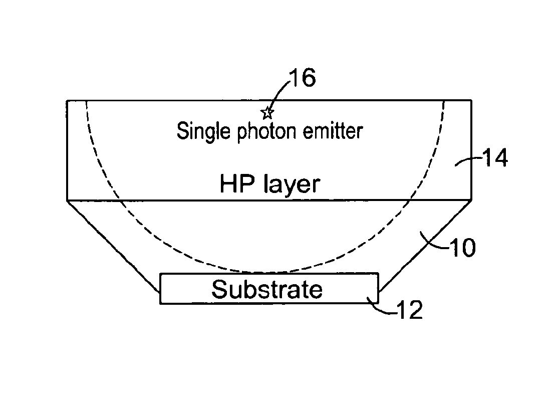
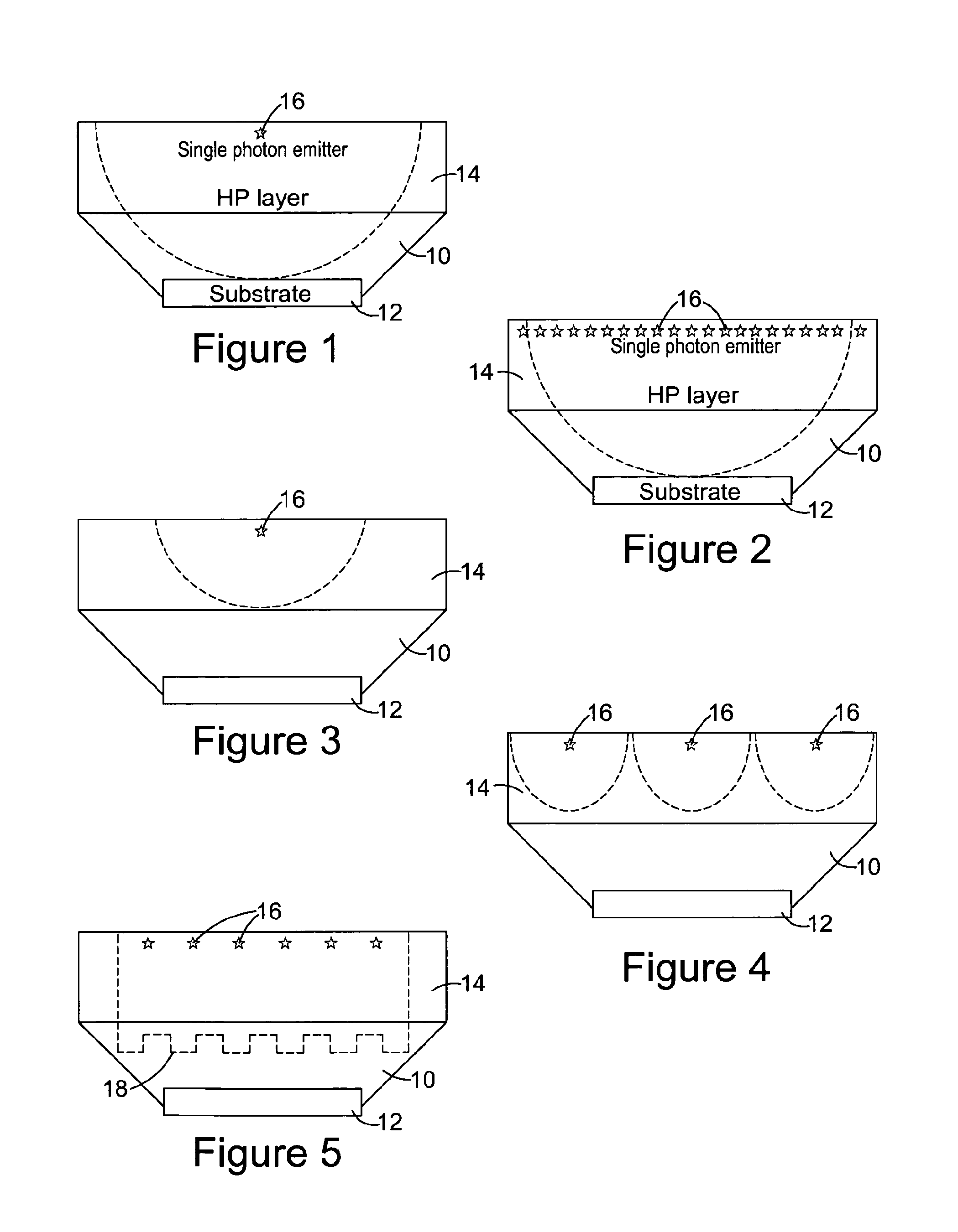
[0016]forming an out-coupling structure at a surface of the optical element for increasing out-coupling of light,

Problems solved by technology

One major problem in producing materials suitable for quantum applications is preventing the qubits from decohering, or at least lengthening the time a system takes to decohere (i.e. lengthening the “decoherence time”).
One problem is that the single photon emission from defects in such materials can be very weak.
Such counting rates might be insufficient for the realization of advanced QIP protocols based on coupling between spin states and optical transitions within reasonable data acquisition times. This problem is also evident for other photon emitting defects within diamond.
In addition to the problem of weak emission, it is evident that the high refractive index of diamond means that due to total internal reflection very few photons can be collected within a small solid angle.
However, single crystal quantum grade diamond material can be difficult, time consuming, and expensive to manufacture, particular for large single crystals, when compared with lower grades of diamond.
As such, it is difficult, time consuming, and costly to form a single crystal quantum grade diamond of sufficient size to incorporate an optical out-coupling structure such as a lens therein.

Method used


Image

  • Diamond optical element
  • Diamond optical element
  • Diamond optical element

Examples


example synthesis

[0105]A synthetic type Ib HPHT diamond plate with a pair of approximately parallel major faces within approximately 5° of (001) was selected. The plate was fabricated into a square substrate suitable for homoepitaxial synthesis of single crystal CVD diamond material by a process including the following steps:

[0106]i) laser cutting of the substrate to produce a plate with all edges;

[0107]ii) lapping and polishing the major surface upon which growth is to occur, the lapped and polished part having dimensions about 3.6 mm×3.6 mm by 535 μm thick, with all faces {100}.

[0108]The defect level at or below the substrate surface is minimised by careful preparation of the substrate as disclosed in EP 1 292 726 and EP 1 290 251. It is possible to reveal the defect levels being introduced by this processing by using a revealing plasma etch. It is possible routinely to produce substrates in which the density of defects measurable after a revealing etch is dependent primarily on the material qual...


PUM

PropertyMeasurementUnit
decoherence time T2aaaaaaaaaa
thicknessaaaaaaaaaa
aspect ratio a/baaaaaaaaaa

Abstract

A method of manufacturing an optical element, the method comprising: growing a first layer of single crystal diamond material via a chemical vapor deposition technique using a gas phase having a first nitrogen concentration; growing a second layer of single crystal diamond material over said first layer via a chemical vapor deposition technique using a gas phase having a second nitrogen concentration, wherein the second nitrogen concentration is lower than the first nitrogen concentration; forming an optical element from at least a portion of the second layer of single crystal diamond material; and forming an out-coupling structure at a surface of the optical element for increasing out-coupling of light.

Description

FIELD OF INVENTION[0001]The present invention relates to diamond optical elements and methods of making the same. The present invention also relates to optical elements comprising a high quality single crystal diamond host material for single photon sources for applications such as magnetometry and quantum information processing.BACKGROUND OF INVENTION[0002]Over the last 20 years there has been substantial interest in the use and manipulation of single photon sources for quantum information processing.[0003]Over the last decade, optically-active defects in diamond have been demonstrated as efficient and robust solid-state single photons sources owing to long decoherence times and strong optical dipole coupling at room temperature. Many optically active defects have been studied in diamond including silicon-vacancy (SiV), nickel and chromium-related defects, and the negatively charged nitrogen-vacancy (NV−) defect. The NV− defect in particular has attracted a lot of interest because ...

Claims


Application Information

Patent Timeline
Patent Type & Authority Patents(United States)
IPC IPC(8): H01J5/16C30B29/04C30B25/02B82Y20/00F21V5/00H01K1/30H01K1/26H01J61/40G02B1/02H01L33/58
CPCF21V5/00B82Y20/00C30B25/02C30B29/04G02B1/02H01L33/58Y10T428/24355Y10T428/24612Y10T428/24628Y10T428/26C01B32/25C23C16/27
Inventor TWITCHEN, DANIEL JAMESDODSON, JOSEPH MICHAELMARKHAM, MATTHEW LEEJELEZKO, FEDOR
Owner ELEMENT SIX TECH LTD
Learn More