Interconnect board and electronic apparatus
a technology of interconnection board and electronic device, which is applied in the direction of cross-talk/noise/interference reduction, electrical apparatus construction details, and incorporation of printed electric components, etc., can solve the problems of noise radiation that has propagated through the conductor, noise leakage outside other layers or multi-layer substrates, and inability to obtain a sufficient noise countermeasure. to prevent the effect of noise radiation
- Summary
- Abstract
- Description
- Claims
- Application Information
AI Technical Summary
Benefits of technology
Problems solved by technology
Method used
Image
Examples
first embodiment
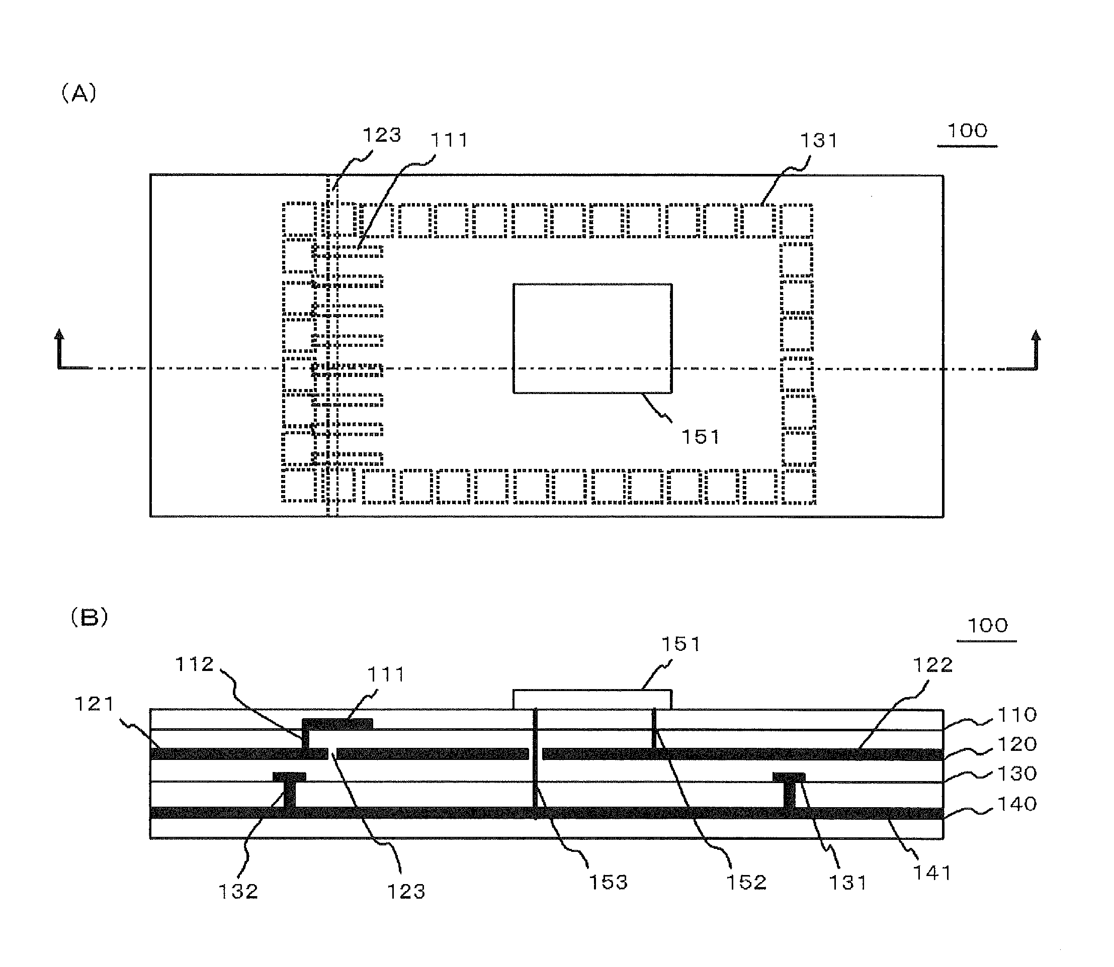
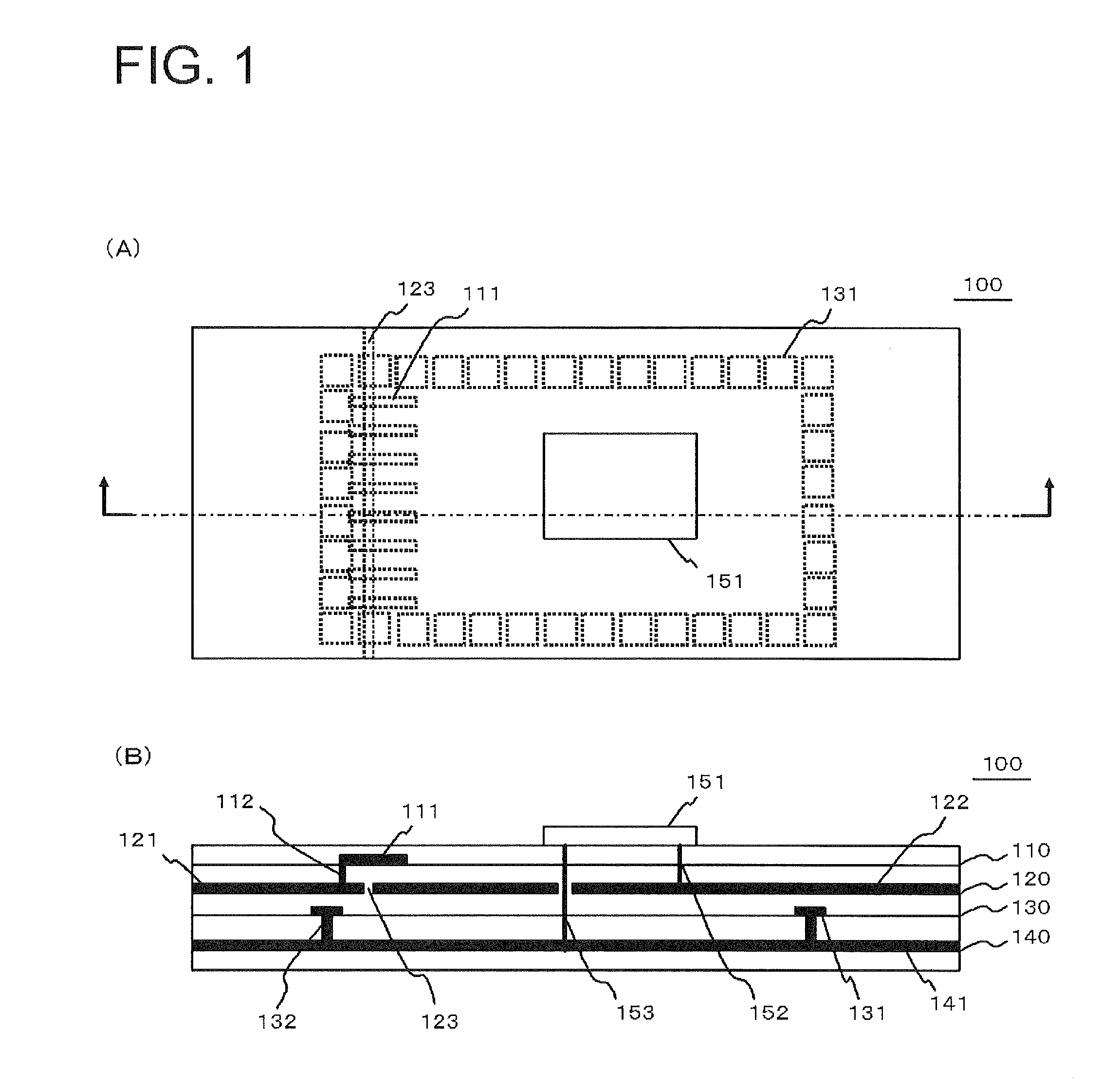
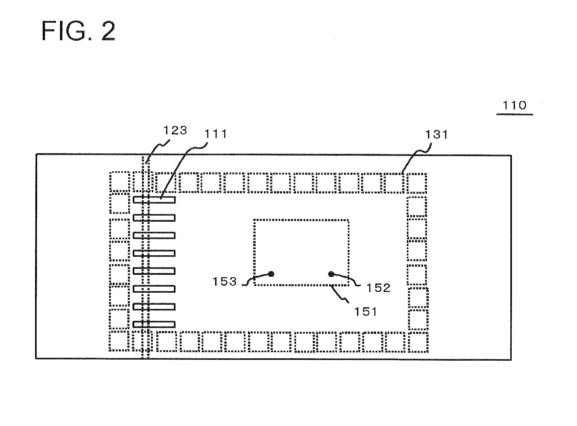
[0029]FIG. 1 shows a top view and a cross-sectional view of an electronic apparatus 100 according to a first embodiment of the invention. More specifically, FIG. 1A is a top view of the electronic apparatus 100, and FIG. 1B is a cross-sectional view of the electronic apparatus 100 at the cross-sectional line shown in FIG. 1A. The electronic apparatus 100 is a multilayer substrate having at least an A layer 110, a B layer 120, a C layer 130, and a D layer 140 sequentially from the top surface.
[0030]Meanwhile, the electronic apparatus 100 may have layers other than the above four layers. For example, the electronic apparatus may have dielectric layers located between the respective layers. In addition, the electronic apparatus 100 may further have holes or via holes, not shown, within the scope of the configuration of the invention. Furthermore, signal wires may be arrayed in the four layers within the scope of the configuration of the invention.
[0031]The electronic apparatus 100 has ...
second embodiment
[0077]FIG. 7 shows a top view and a cross-sectional view of the electronic apparatus 100 according to a second embodiment of the invention. In more detail, FIG. 7A is a top view of the electronic apparatus 100, and FIG. 7B is a cross-sectional view of the electronic apparatus 100 at the cross-sectional line shown in FIG. 7A.
[0078]Compared to the electronic apparatus 100 of the first embodiment, the electronic apparatus 100 of the embodiment does not have the plurality of open stubs 111 and the A layer 110 on which the open stubs are located, and the difference is that, instead, a pectinate protrusion portion 124 is disposed at the gap 123 between the power supply plane 121 and the power supply plane 122. In other words, a plurality of recess portions are formed on a side facing the gap 123 in the power supply plane 122, and the protrusion portion 124 integrally formed with the power supply plane 121 is inserted into the respective plurality of recess portions.
[0079]FIG. 8 is a view ...
PUM
 Abstract
Description
Claims
Application Information
 - R&D
- Intellectual Property
- Life Sciences
- Materials
- Tech Scout
- Unparalleled Data Quality
- Higher Quality Content
- 60% Fewer Hallucinations
Browse by: Latest US Patents, China's latest patents, Technical Efficacy Thesaurus, Application Domain, Technology Topic, Popular Technical Reports.
© 2025 PatSnap. All rights reserved.Legal|Privacy policy|Modern Slavery Act Transparency Statement|Sitemap|About US| Contact US: help@patsnap.com


