Method for improving write margins of SRAM cells

a technology of sram cells and write margins, which is applied in the direction of semiconductor devices, electrical apparatus, transistors, etc., can solve the problems of unsatisfactory write margin of sram cells manufactured by the conventional sram fabrication method, and achieve the effect of improving the write margin of sram cells, increasing the equivalent resistance of pull up mos, and increasing the write margin

Active Publication Date: 2014-09-02
SHANGHAI HUALI MICROELECTRONICS CORP
View PDF3 Cites 0 Cited by
  • Summary
  • Abstract
  • Description
  • Claims
  • Application Information

AI Technical Summary

Benefits of technology

[0007]Accordingly, at least one object of the present invention is to provide a method to enhance the write margins of the SRAM cells effectively, and a method for manufacturing the SRAM cells with enhanced write margins.
[0008]According to the first aspect of the present invention, there is provided a method for improving the write margins of the SRAM cells comprising: before etching a polysilicon layer to form the polysilicon gates, performing a pre-implantation process to the polysilicon layer; wherein the polysilicon layer defines SRAM NMOSFETs regions and SRAM PMOSFETs regions; the pre-implantation process comprises pre-implanting the fifth-group elements to the SRAM NMOSFETs regions and the NMOSFETs regions except to the SRAM NMOSFETs regions in the polysilicon layer, and pre-implanting the third-group elements to the PMOSFETs regions excluding the SRAM PMOSFETs regions in the polysilicon layer; wherein the process of pre-implanting the third-group elements comprises forming a pre-implantation photo mask capable of covering the SRAM PMOSFETs regions and using the pre-implantation photo mask to pre-implanting the third-group elements.
[0013]According to the second aspect of the present invention, a method for manufacturing SRAM cells with enhanced write margins is provided. The method comprises: depositing a polysilicon layer in which SRAM NMOSFETs regions and SRAM PMOSFETs regions are defined; Pre-implanting the fifth-group elements to the SRAM NMOSFETs regions as well as the other NMOSFETs regions in the polysilicon layer except to the SRAM NMOSFETs regions; Pre-implanting the third-group elements to the other PMOSFETs regions excluding the SRAM PMOSFETs regions in the polysilicon layer by using a pre-implantation photo mask covering the SRAM PMOSFETs regions.
[0014]In the present invention, the process of pre-implanting the Pull Up MOS regions of the SRAM is removed by using a designed pre-implantation photo mask, and thus the doping concentration of the polysilicon gate of the Pull Up MOS is reduced, the equivalent resistance of the Pull Up MOS is increased, and the write margin of the SRAM cell is improved.

Problems solved by technology

However, the write margin of the SRAM cell which is manufactured by the conventional SRAM fabrication method is not satisfying.

Method used


Image

  • Method for improving write margins of SRAM cells
  • Method for improving write margins of SRAM cells
  • Method for improving write margins of SRAM cells

Examples


Embodiment Construction

[0019]Reference will now be made in detail to the present preferred embodiments and the accompanying figures of the invention in order to provide a further understanding of the invention. The figures are not drawn to scale and they are provided merely to illustrate the invention instead of limiting the scope of the present invention, like reference numerals are used throughout the figures to designate similar or equivalent element.

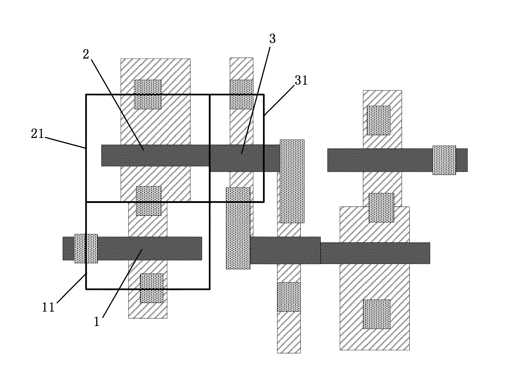
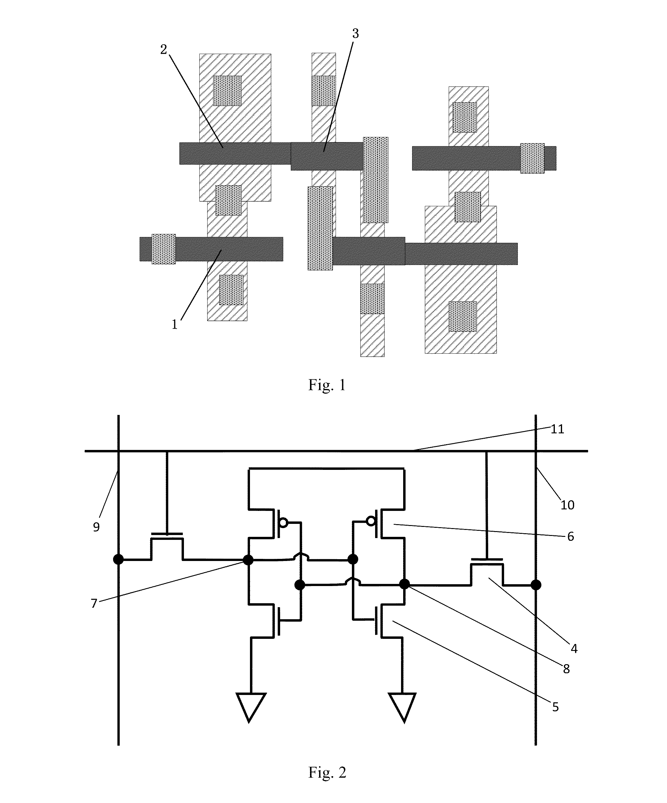
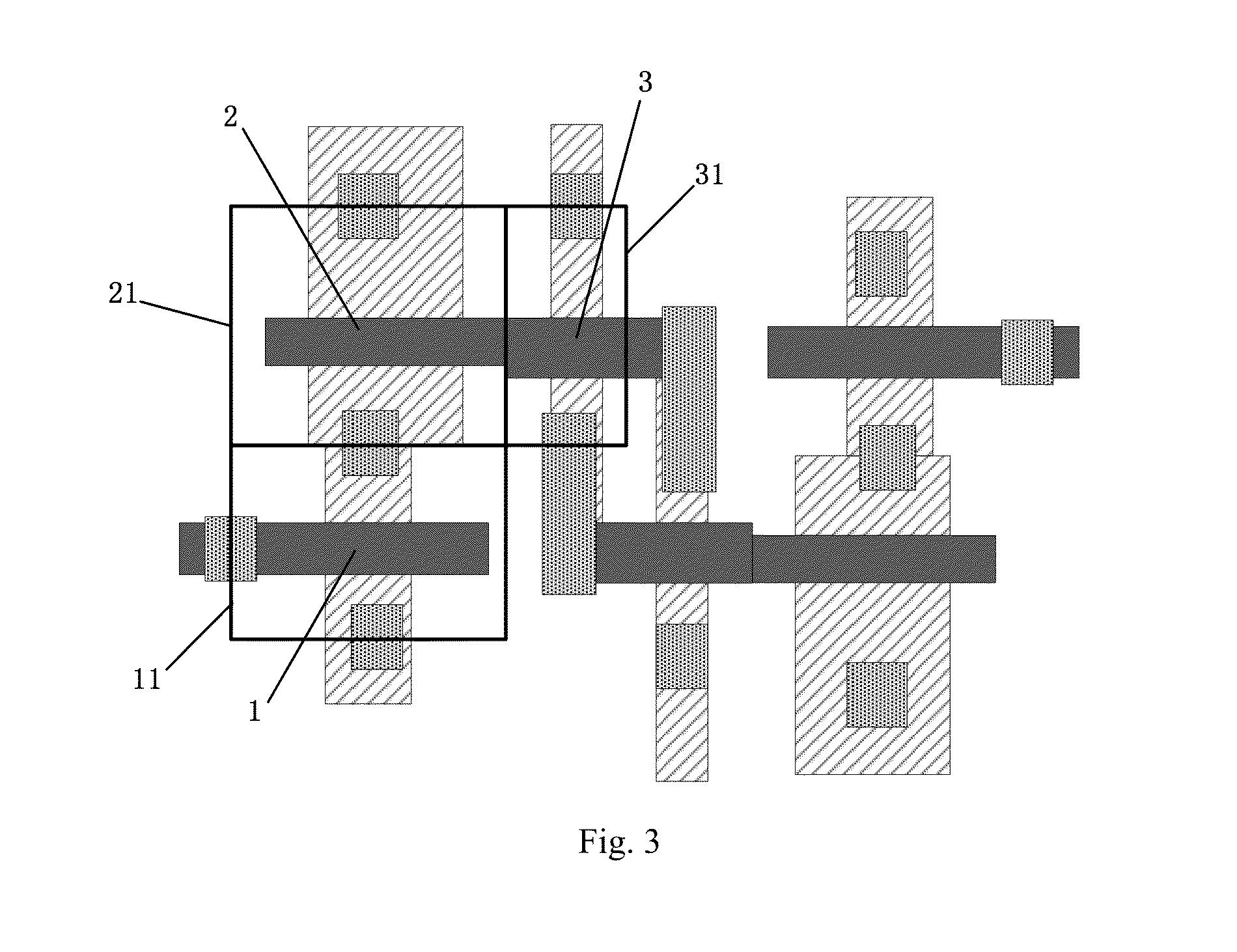
[0020]FIG. 3 is a schematic diagram of the layout of the SRAM cell with enhanced write margins in an embodiment of the present invention.

[0021]In an embodiment, the method for improving the write margins of the SRAM cells comprises: before etching a polysilicon layer to form the polysilicon gates, performing a pre-implantation process to the polysilicon layer, wherein the polysilicon layer defines SRAM NMOSFETs regions and SRAM PMOSFETs regions. The polysilicon gates can be the polysilicon gates of different semiconductor devices. The pre-implantation proc...


PUM


Abstract

The present invention provides a method for improving the write margins of the SRAM cells. The method comprises: before etching a polysilicon layer to form the polysilicon gates, performing a pre-implantation process to the polysilicon layer; wherein the polysilicon layer defines SRAM NMOSFETs regions and SRAM PMOSFETs regions; wherein the pre-implantation process comprises pre-implanting the fifth-group elements to the SRAM NMOSFETs regions and the NMOSFETs regions except to the SRAM NMOSFETs regions in the polysilicon layer, and pre-implanting the third-group elements to the PMOSFETs regions excluding the SRAM PMOSFETs regions in the polysilicon layer; wherein the process of pre-implanting the third-group elements comprises forming a pre-implantation photo mask capable of covering the SRAM PMOSFETs regions and using the pre-implantation photo mask to pre-implanting the third-group elements.

Description

CROSS-REFERENCE TO RELATED APPLICATION[0001]This application claims the priority benefit of China application serial no. 201210093940.0, filed Mar. 31, 2012. All disclosure of the China application is incorporated herein by reference.FIELD OF THE INVENTION[0002]The present invention relates to the field of semiconductor fabrication technology and particularly to a method for improving the write margins of the SRAM cells and a method for manufacturing the SRAM cells with enhanced write margins.BACKGROUND OF THE INVENTION[0003]The SRAM (static random access memory) is an important semiconductor memory and is widely used in the high-speed data exchange systems such as the computers, communications, multimedia, etc. FIG. 1 illustrates a layout structure of a SRAM cell less than 90 nm. As shown in FIG. 1, the layout structure of a SRAM cell comprises three portions including the active areas, the polysilicon gates and the contact holes. Wherein the numeral 1 represents a Pass Gate, which...

Claims


Application Information

Patent Timeline
Patent Type & Authority Patents(United States)
IPC IPC(8): H01L21/00H01L21/28H01L27/02H01L27/11
CPCH01L21/28H01L27/1104H01L27/0207H10B10/12
Inventor YU, LIUJIANG
Owner SHANGHAI HUALI MICROELECTRONICS CORP
Why Eureka
Try Eureka