
Display element having a lens being formed as part of a translucent support substrate having a display disposed thereon

a technology of electronic elements and lenses, which is applied in the field of display elements and electronic element modules, can solve the problems of reducing the installation area, thinning the terminal, and the inability to achieve a further reduction of so as to reduce the installation area, reduce the number of parts, and reduce the effect of thinning the terminal

Inactive Publication Date: 2014-04-22
SHARP KK
View PDF4 Cites 2 Cited by
  • Summary
  • Abstract
  • Description
  • Claims
  • Application Information

AI Technical Summary

Benefits of technology

[0022]Even in the conventional integrated structure of a display element and an image capturing element disclosed in Reference 2 described above, it is not possible to achieve a further reduction of the number of parts, a reduction of the installing area, downsizing and thinning of the terminal by the improvement of the wiring efficiency, or lowering of the power consumption.
[0023]The present invention is intended to solve the conventional problems described above. The objective of the present invention is to provide a display element and electronic element module, such as an image capturing element with an integrated display element, which has a structure, in which an image capturing element and even a lens are integrated on a glass substrate having a display element disposed thereon, so as to achieve a further reduction of the number of parts, a reduction of the installing area, downsizing and thinning of the terminal by the improvement of the wiring efficiency, and lowering of the power consumption; a method for manufacturing the display element and electronic element module; and an electronic information device, such as a camera-equipped cell phone device, having the display element and electronic element module used in a display section and a light receiving section thereof.

Problems solved by technology

Even in the conventional integrated structure of a display element and an image capturing element disclosed in Reference 2 described above, it is not possible to achieve a further reduction of the number of parts, a reduction of the installing area, downsizing and thinning of the terminal by the improvement of the wiring efficiency, or lowering of the power consumption.

Method used


Image

  • Display element having a lens being formed as part of a translucent support substrate having a display disposed thereon
  • Display element having a lens being formed as part of a translucent support substrate having a display disposed thereon
  • Display element having a lens being formed as part of a translucent support substrate having a display disposed thereon

Examples


embodiment 4

[0166]Hereinafter, as Embodiments 1 to 3 of a display element and electronic element module and a method for manufacturing the display element and electronic element module according to the present invention, a display element and image capturing element module, such as a liquid crystal display module with an integrated light receiving section, and a method for manufacturing thereof will be described in detail with reference to accompanying figures; and as Embodiment 4, an electronic information device, such as a camera-equipped cell phone device, having the display element and electronic element module used in a display section and an image capturing section, as a light receiving section thereof, will be described in detail with reference to accompanying figures.

embodiment 1

[0167](Embodiment 1)

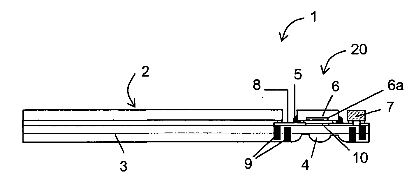
[0168]FIG. 1 is a longitudinal cross sectional view illustrating an exemplary essential structure of a display element and electronic element module according to Embodiment 1 of the present invention. FIG. 2 is an enlarged cross sectional view of an image capturing element portion of FIG. 1.

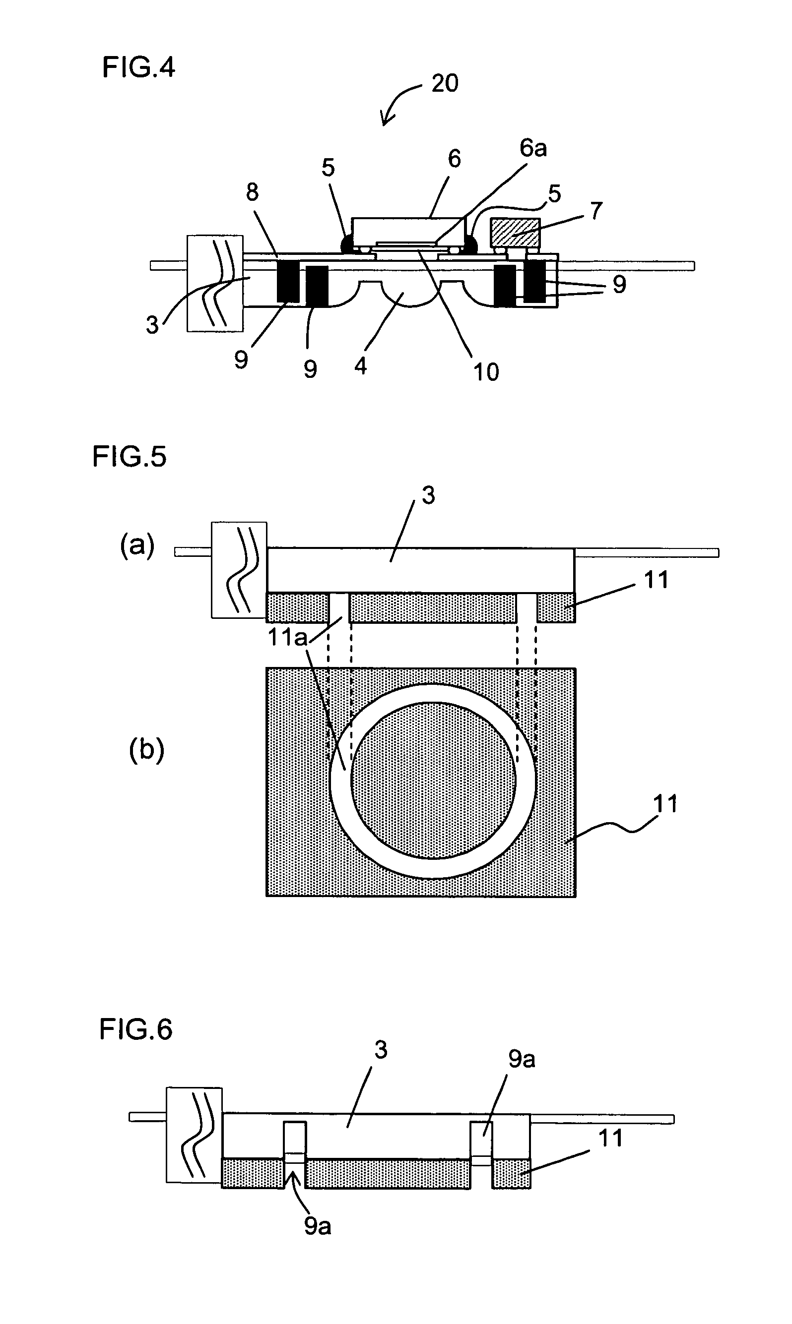
[0169]In FIGS. 1 and 2, a display element and image capturing element module 1 according to Embodiment 1 is an image capturing element with an integrated display element (a display module with an integrated light receiving element). The display element and image capturing element module 1 includes: a display apparatus 2 disposed on a glass substrate 3; a lens 4 having a curved surface on a surface opposite from a surface with the display apparatus 2; lens shielding layers 9 and 9 having a double circular shape in a plan view, for shielding an outer circumference side of the lens 4 in a plan view; an image capturing element 6 disposed by sealing the periphery of a chip by a shi...

embodiment 2

[0197](Embodiment 2)

[0198]In Embodiment 1 described above, a case has been described where the direction of the display screen of the display apparatus 2 is opposite from the direction in which the image capturing element module 20 captures an image. In Embodiment 2, a case will be described where the direction of the display image of the display apparatus 2 is the same as the direction in which an image capturing element module 20C, which will be described later, takes in incident light and captures an image.

[0199]FIG. 31 is a longitudinal cross sectional view illustrating an exemplary essential structure of a display element and image capturing element module according to Embodiment 2 of the present invention.

[0200]In FIG. 31, a display element and image capturing element module 1A according to Embodiment 2 is an image capturing element with an integrated display element. The display element and image capturing element module 1A includes: a display apparatus 2 disposed on a glass ...


PUM

PropertyMeasurementUnit
temperatureaaaaaaaaaa
sizeaaaaaaaaaa
thicknessaaaaaaaaaa

Abstract

A display element and electronic element module according to the present invention is described, in which a lens is formed as part of a translucent support substrate having a display disposed thereon, the lens being formed on a part other than where the display is disposed, where an electronic element is disposed for the lens.

Description

[0001]This nonprovisional application claims priority under 35 U.S.C. §119(a) to Patent Application No. 2008-206440 filed in Japan on Aug. 8, 2008, the entire contents of which are hereby incorporated by reference.BACKGROUND OF THE INVENTION[0002]1. Field of the Invention[0003]The present invention relates to a display element and electronic element module, such as a display module with an integrated light receiving element, in which an image capturing element is integrated with a glass substrate functioning as a transparent support substrate having a display element disposed thereon, the image capturing element being configured with a semiconductor element for performing a photoelectric conversion on and capturing an image from an image light from a subject; and a method for manufacturing the display element and electronic element module. Furthermore, the present invention relates to an electronic information device, such as a digital camera (e.g., a digital video camera and a digi...

Claims


Application Information

Patent Timeline
Patent Type & Authority Patents(United States)
IPC IPC(8): G03B17/02G02F1/13G02F1/1333G03B17/18G03B13/02G03B17/00G02F1/1345G03B29/00
CPCG02F1/133526H04N5/2253H01L27/14625H01L27/14601H04N23/54
Inventor OKITA, YOSHITAKATAKATA, HIDEKAZUIMANISHI, MASATOFUJITA, KAZUYA
Owner SHARP KK
Learn More