Antenna apparatus including feeding elements and parasitic elements activated as reflectors
a technology of antenna apparatus and parasitic elements, applied in the structure of radiating elements, elongated active elements, resonance antennas, etc., can solve the problems of lowering transmission quality, and achieve the effect of neglecting propagation loss, increasing and reducing radiation power
- Summary
- Abstract
- Description
- Claims
- Application Information
AI Technical Summary
Benefits of technology
Problems solved by technology
Method used
Image
Examples
first preferred embodiment
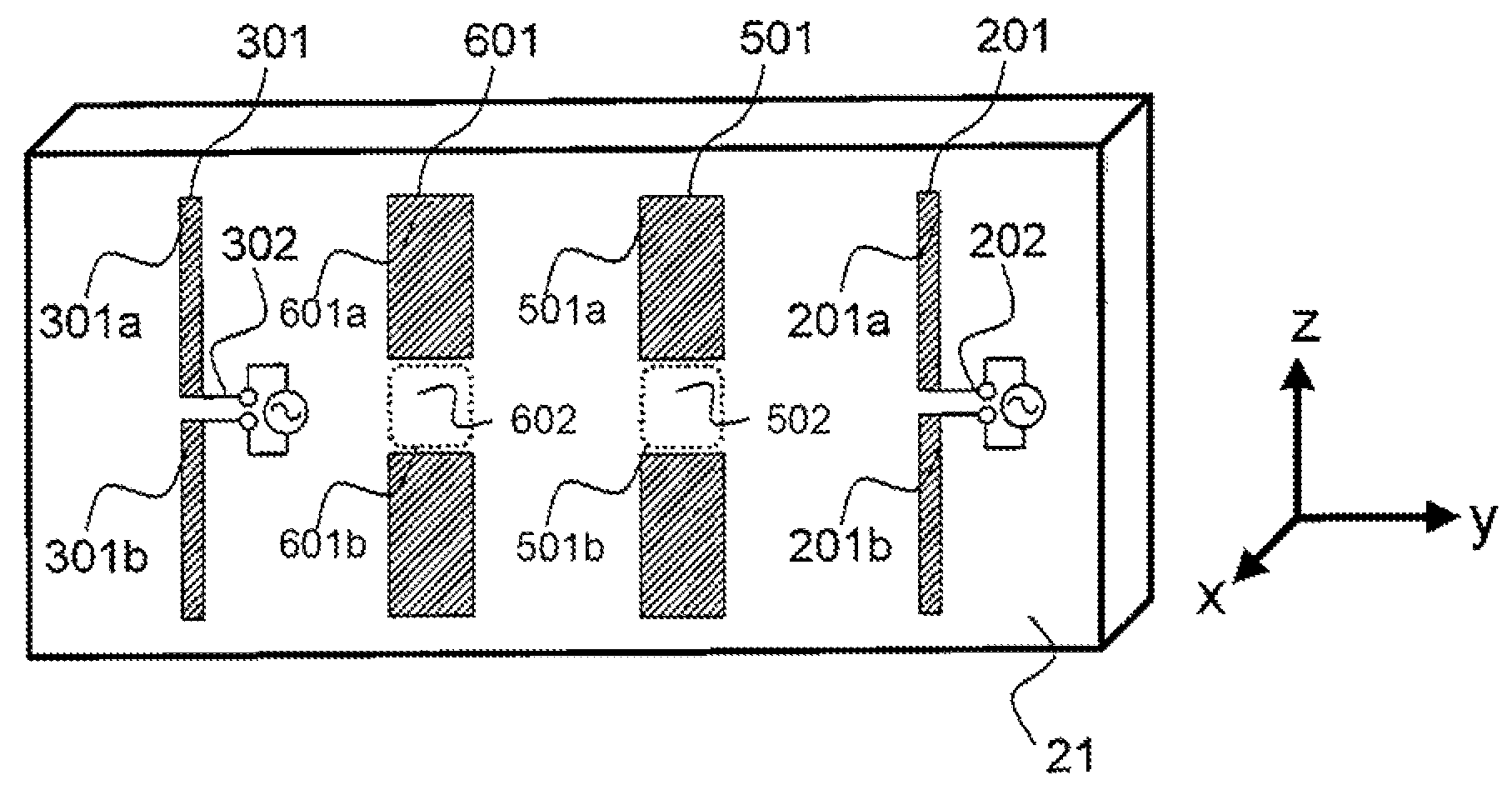
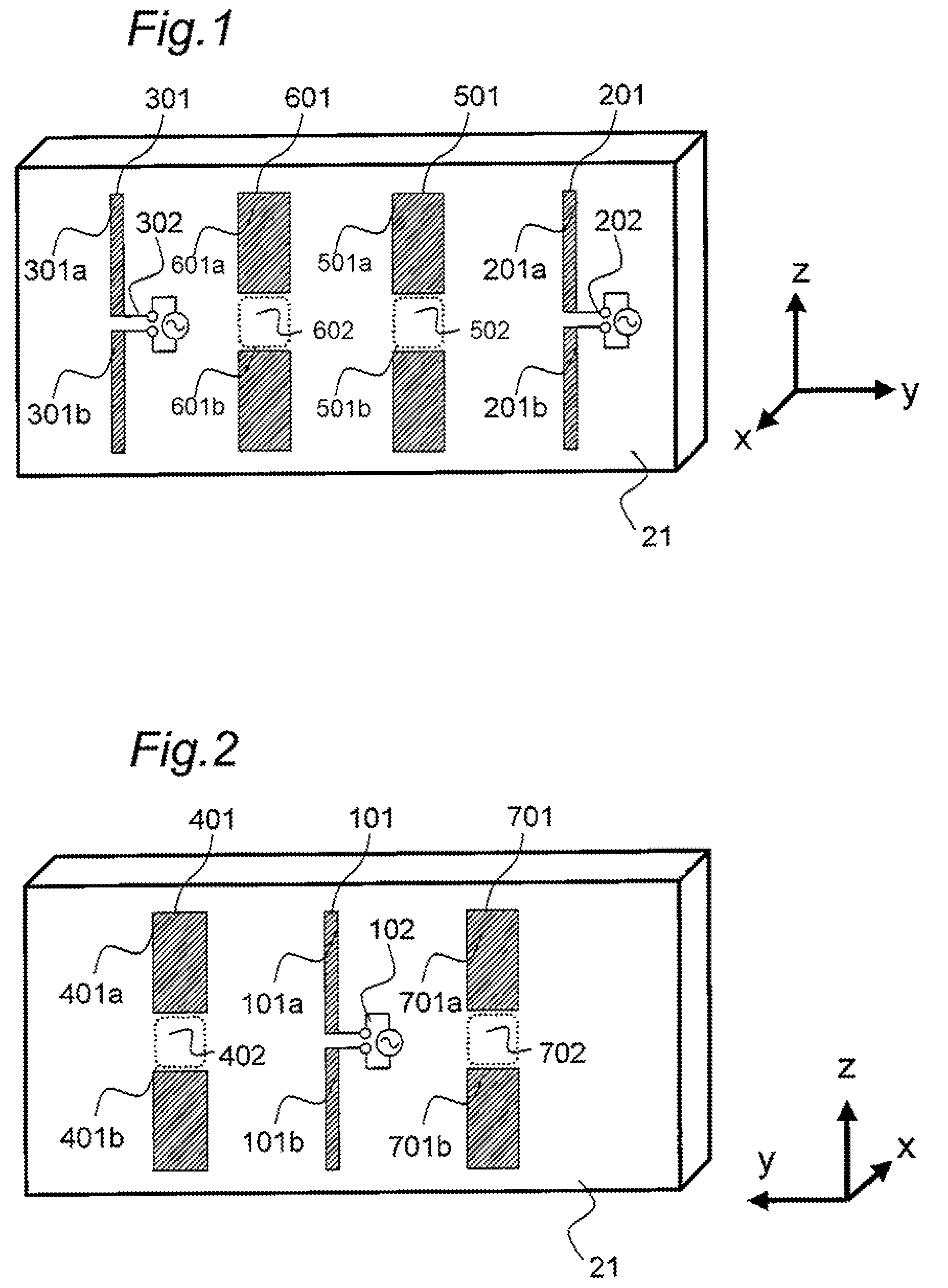
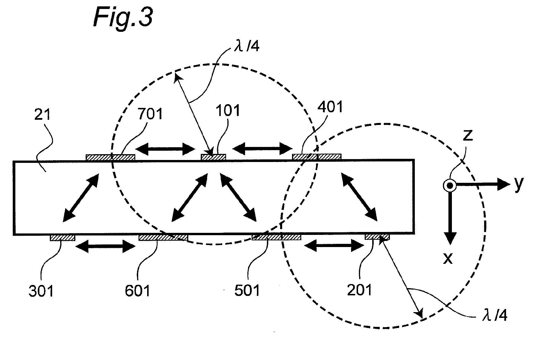
[0055]FIG. 1 is a perspective view when an antenna apparatus according to a first preferred embodiment of the present invention is seen from a front side thereof, and FIG. 2 is a perspective view when the antenna apparatus of FIG. 1 is seen from a back side thereof. In addition, FIG. 3 is a top view of the antenna apparatus of FIGS. 1 and 2. The antenna apparatus according to the present preferred embodiment is configured to include three dipole antenna elements 101, 201 and 301, and four parasitic antenna elements (that are parasitic elements) 401, 501, 601 and 701 each provided on a dielectric substrate 21. In addition, a three-dimensional XYZ coordinate is adopted as shown in FIGS. 1 to 3.
[0056]As will be described later in detail, the antenna apparatus according to the present preferred embodiment has the following features. Namely, the antenna apparatus includes the dielectric substrate 21, the feeding antenna element 101 formed on one surface of the dielectric substrate 21 to ...
second preferred embodiment
[0077]FIG. 8 is a perspective view of an antenna apparatus according to a second preferred embodiment of the present invention. In addition, FIG. 9 is a front view of a printed circuit board 22a according to the second preferred embodiment of the present invention, and FIG. 10 is a front view of a printed circuit board 22b according to the second preferred embodiment of the present invention.
[0078]As shown in FIG. 8, the antenna apparatus of the present preferred embodiment is configured to include the two printed circuit boards 22a and 22b formed by dielectric, which are provided in parallel with each other and arranged along a portion of a notch of a metal housing 23 of a display, where the notch has a plastic window 24 incorporated therein. In this case, the printed circuit board 22a has a first surface 22a-s1 and a second surface 22a-s2 which are in parallel with each other, and the printed circuit board 22b has a first surface 22b-s1 and a second surface 22b-s2 which are in par...
third preferred embodiment
[0089]FIG. 17 is a perspective view showing a schematic configuration of a wireless module substrate 25 provided with an antenna apparatus according to a third preferred embodiment of the present invention. In addition, FIG. 18 is a perspective view when a dielectric substrate 21 of FIG. 17 is seen from a front side thereof, FIG. 19 is a perspective view when the dielectric substrate 21 of FIG. 17 is seen from a back side thereof, and FIG. 20 is a perspective view when the dielectric substrate 21 of FIG. 17 is seen from a bottom side thereof. In this case, FIG. 17 shows a type of usage of the antenna apparatus according to the third preferred embodiment of the present invention.
[0090]Referring to FIGS. 17 to 20, the antenna apparatus of the present preferred embodiment is configured to include three monopole antenna elements 101B, 201B and 301B and four parasitic antenna elements 401A, 501A, 601A and 701A provided on the dielectric substrate 21. The monopole antenna element 101B and...
PUM
 Abstract
Description
Claims
Application Information
 - R&D
- Intellectual Property
- Life Sciences
- Materials
- Tech Scout
- Unparalleled Data Quality
- Higher Quality Content
- 60% Fewer Hallucinations
Browse by: Latest US Patents, China's latest patents, Technical Efficacy Thesaurus, Application Domain, Technology Topic, Popular Technical Reports.
© 2025 PatSnap. All rights reserved.Legal|Privacy policy|Modern Slavery Act Transparency Statement|Sitemap|About US| Contact US: help@patsnap.com


