
Transistor

a transistor and field-effect technology, applied in the field of field-effect transistors, can solve the problems of low threshold voltage, high threshold voltage, and high potential leakage current, and achieve the effect of increasing purity and low off-state curren

Inactive Publication Date: 2013-12-03
SEMICON ENERGY LAB CO LTD
View PDF155 Cites 3 Cited by
  • Summary
  • Abstract
  • Description
  • Claims
  • Application Information

AI Technical Summary

Benefits of technology

[0010]In order to increase field-effect mobility of a thin film transistor, the channel length along which carriers transfer is preferably small. However, when the channel length is small, off-state current of the thin film transistor is increased.
[0011]Thus, it is an object of one embodiment of the present invention to provide a thin film transistor with high speed operation, in which a large mount of current can flow when the thin film transistor is on and off-state current is extremely reduced when the thin film transistor is off.
[0016]According to one embodiment of the present invention, an oxide semiconductor whose hydrogen concentration is reduced and purity is increased is used, so that field-effect mobility and an on-state current of the field-effect transistor, for example the thin film transistor can be improved, and very low off-state current can be obtained.

Problems solved by technology

In the display device, there is a problem in that unwanted charge build-up is caused in elements, electrodes, or wirings during manufacture or operation.
Further, in the case where a bottom gate transistor is used, charge may build up on a surface of or in a back channel portion in a semiconductor layer (i.e., a region of a semiconductor layer which is sandwiched between a source electrode and a drain electrode which are formed over the semiconductor layer) and generate a parasitic channel, so that leakage current is likely to occur and threshold voltage varies.

Method used


Image

  • Transistor
  • Transistor
  • Transistor

Examples


embodiment 1

(Embodiment 1)

[0036]In this embodiment, a structure of a field-effect transistor, for example a thin film transistor will be described with reference to FIGS. 1A and 1B.

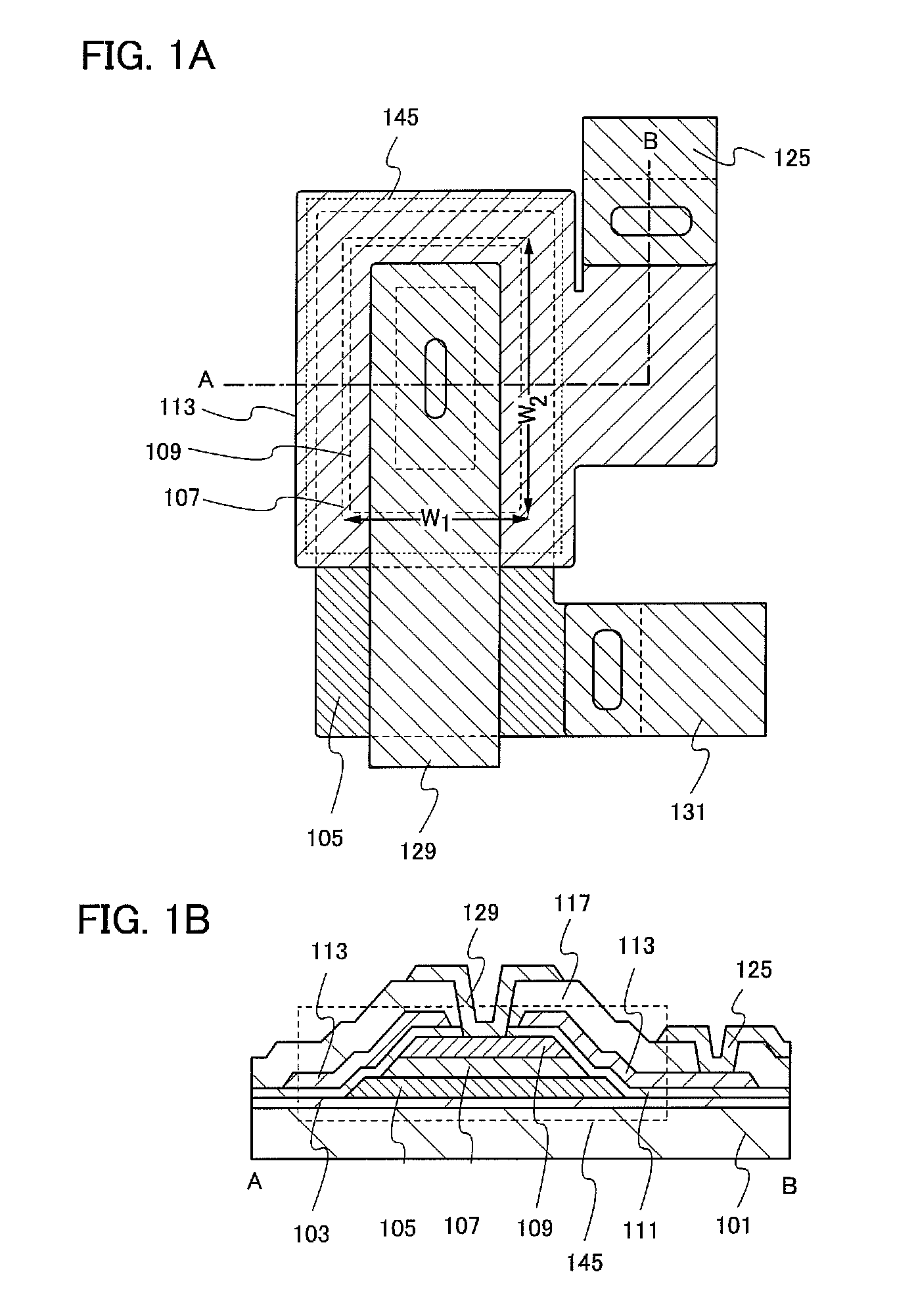
[0037]FIG. 1A is a top view of a thin film transistor 145, and FIG. 1B corresponds to a cross-sectional view of dashed line A-B of FIG. 1A.

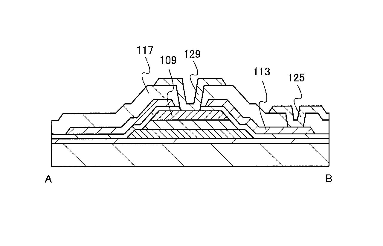
[0038]As illustrated in FIG. 1B, a first electrode 105, an oxide semiconductor film 107, and a second electrode 109 are stacked over an insulating film 103 formed over a substrate 101. A gate insulating film 111 is provided so as to cover the first electrode 105, the oxide semiconductor film 107, and the second electrode 109. A third electrode 113 is provided over the gate insulating film 111. An insulating film 117 functioning as an interlayer insulating film is provided over the gate insulating film 111 and the third electrode 113. Openings are formed in the insulating film 117, and a wiring 131 (see FIG. 1A) connected via the opening to the first electrode 105, a wiring 129 con...

embodiment 2

(Embodiment 2)

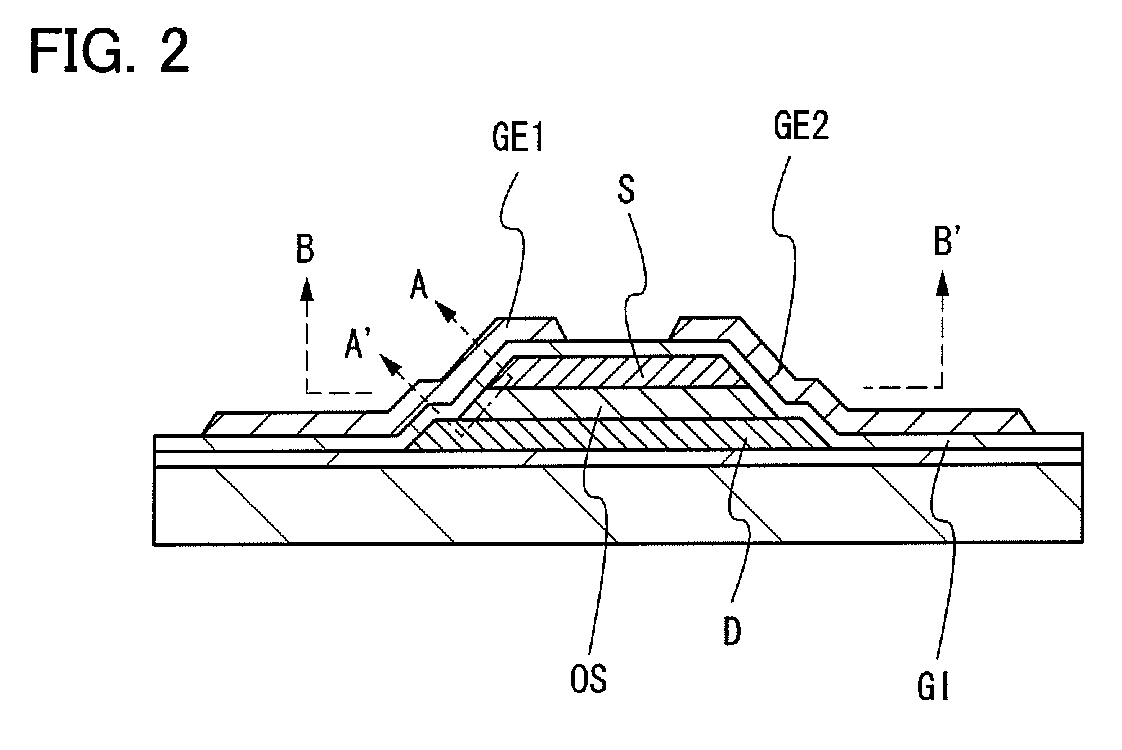
[0072]In this embodiment, a structure of a field-effect transistor, for example a thin film transistor, which is different from that of the thin film transistor described in Embodiment 1, will be described with reference to FIGS. 6A and 6B.

[0073]FIG. 6A is a top view of thin film transistors 147 and 149, and FIG. 6B corresponds to a cross-sectional view taken along chain line A-B in FIG. 6A.

[0074]As illustrated in FIG. 6B, the first electrode 105 and a first electrode 106, the oxide semiconductor film 107, and the second electrode 109 are stacked over the insulating film 103 formed over the substrate 101. The gate insulating film 111 is provided so as to cover the first electrodes 105 and 106, the oxide semiconductor film 107, and the second electrode 109. The third electrode 113 is provided over the gate insulating film 111. The insulating film 117 functioning as an interlayer insulating film is provided over the gate insulating film 111 and the third electrode 113. O...

embodiment 3

(Embodiment 3)

[0078]In this embodiment, a manufacturing process of the thin film transistor in FIGS. 1A and 1B will be described with reference to FIGS. 7A to 7E.

[0079]As illustrated in FIG. 7A, the insulating film 103 is formed over the substrate 101, and the first electrode 105 is formed over the insulating film 103. The first electrode 105 functions as one of the source electrode and the drain electrode of the thin film transistor.

[0080]The insulating film 103 can be formed by a sputtering method, a CVD method, a coating method, or the like.

[0081]Note that when the insulating film 103 is formed by a sputtering method, the insulating film 103 is preferably formed while hydrogen, water, hydroxyl groups, hydride, or the like remaining in a treatment chamber is removed. This is for preventing hydrogen, water, hydroxyl groups, hydride, or the like from being contained in the insulating film 103. It is preferable to use an entrapment vacuum pump in order to remove hydrogen, water, hydr...


PUM


Abstract

It is an object to provide a thin film transistor with high speed operation, in which a large amount of current can flow when the thin film transistor is on and off-state current is extremely reduced when the thin film transistor is off. The thin film transistor is a vertical thin film transistor in which a channel formation region is formed using an oxide semiconductor film in which hydrogen is contained in an oxide semiconductor at a concentration of lower than or equal to 5×10¹⁹ / cm3, preferably lower than or equal to 5×10¹⁸ / cm3, more preferably lower than or equal to 5×10¹⁷ / cm3, hydrogen or an OH group contained in the oxide semiconductor is / are removed, and carrier concentration is lower than or equal to 5×10¹⁴ / cm3, preferably lower than or equal to 5×10¹² / cm3.

Description

TECHNICAL FIELD[0001]The present invention relates to a field-effect transistor, for example a thin film transistor formed using an oxide semiconductor.BACKGROUND ART[0002]A lot of attention has been paid to the technology of forming a field-effect transistor, for example a thin film transistor (TFT), by using a semiconductor thin film that is formed over a substrate having an insulating surface. The thin film transistor is used for a display device typified by a liquid crystal television. Although silicon-based semiconductor material is known as a material for a semiconductor thin film which can be applied to the thin film transistor, an oxide semiconductor has attracted attention as another material.[0003]As the material for the oxide semiconductor, zinc oxide and a material containing zinc oxide are known. A thin film transistor formed using an amorphous oxide (oxide semiconductor) whose electronic carrier concentration is lower than 1018 / cm3 is disclosed (Patent Documents 1 to 3...

Claims


Application Information

Patent Timeline
Patent Type & Authority Patents(United States)
IPC IPC(8): H01L29/76
CPCH01L27/1225H01L29/41733H01L29/42392H01L29/78606H01L29/78642H01L29/7869H01L29/78696
Inventor YAMAZAKI, SHUNPEI
Owner SEMICON ENERGY LAB CO LTD
Learn More