Light guide plate and backlight module having high light utilization efficiency by reducing light loss
a technology of light guide plate and backlight module, which is applied in the field of optical elements and light sources, can solve the problems of reducing the light utilization efficiency increasing the material cost of the backlight module, and unable to enable the light beam to exit in a desired angle, so as to reduce the light loss
- Summary
- Abstract
- Description
- Claims
- Application Information
AI Technical Summary
Benefits of technology
Problems solved by technology
Method used
Image
Examples
first embodiment
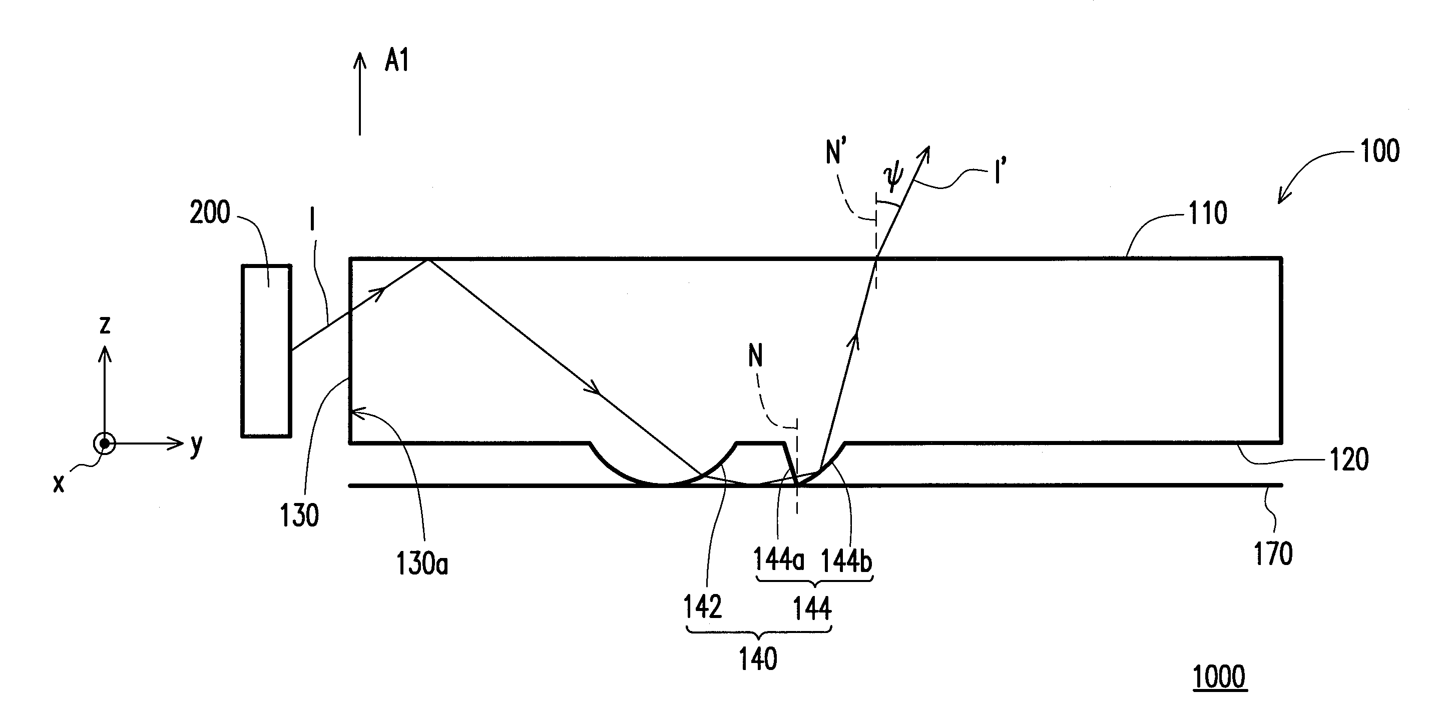
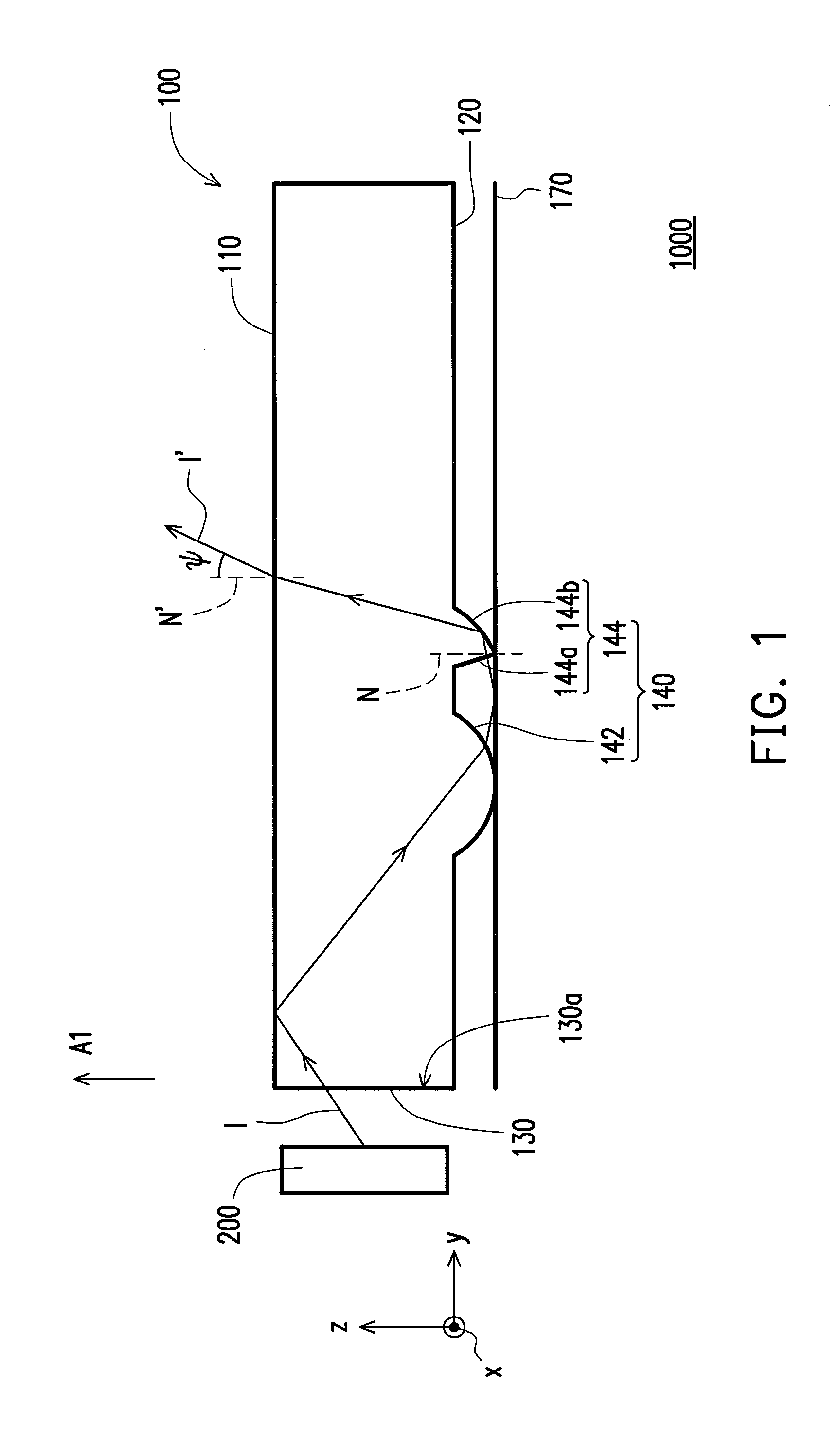
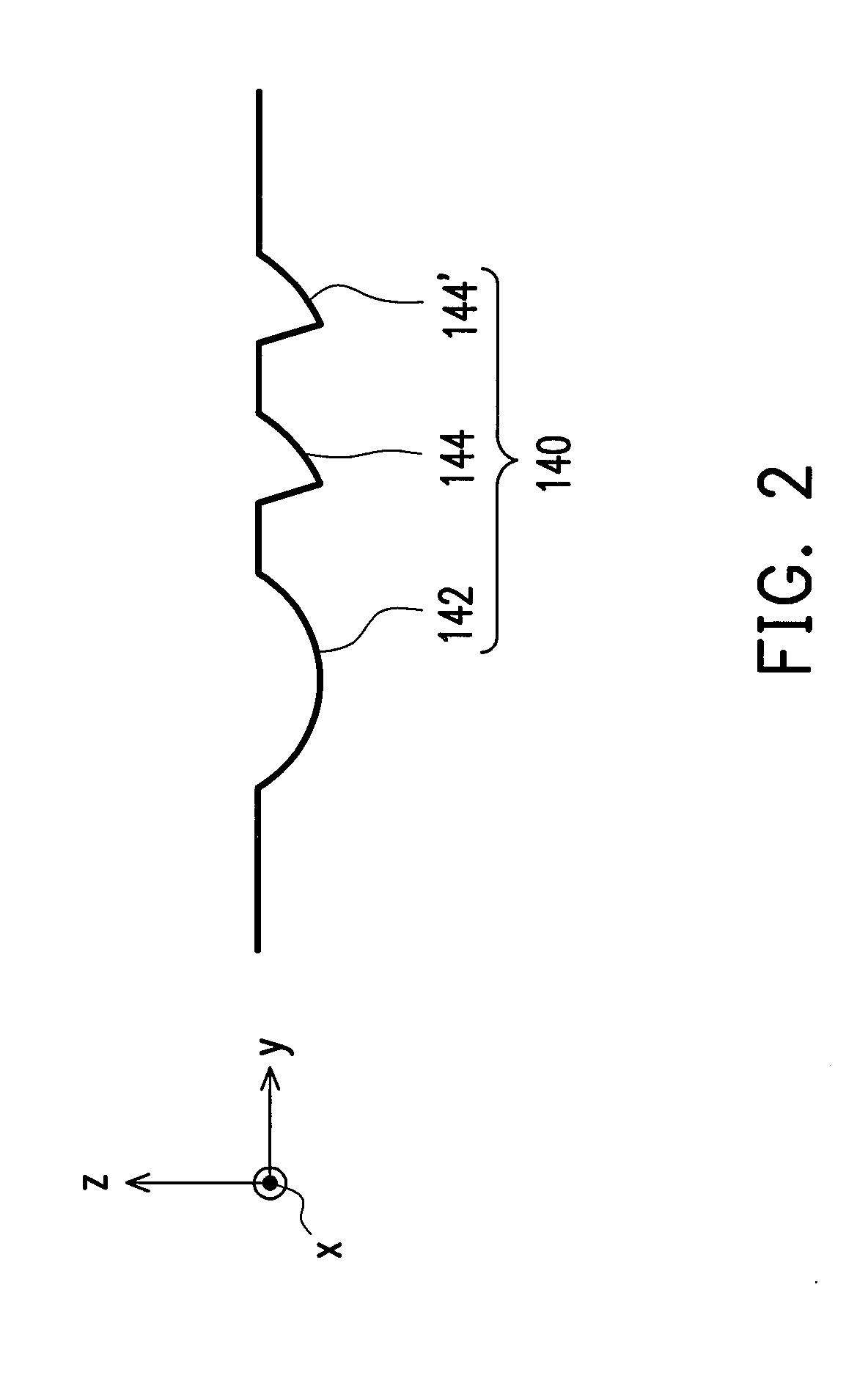
[0035]FIG. 1 is a schematic sectional view of a backlight module according to a first embodiment of the invention. Referring to FIG. 1, a backlight module 1000 of this embodiment includes a light guide plate 100 and at least one light-emitting element 200. The light guide plate 100 of this embodiment includes a light emitting surface 110 (for example, a plane parallel to an xy plane), a bottom surface 120 (for example, the xy plane) opposite to the light emitting surface 110, a light incident surface 130 (for example, a plane parallel to an xz plane) connecting the light emitting surface 110 and the bottom surface 120, and a plurality of optical units 140 disposed on the bottom surface 120 (only one optical unit 140 is exemplarily illustrated in FIG. 1, and is used as a representative). The backlight module 1000 of this embodiment may further include a reflective sheet 170. The bottom surface 120 is between the reflective sheet 170 and the light emitting surface 110. The reflective ...
second embodiment
[0047]FIG. 7 is a schematic sectional view of a backlight module according to a second embodiment of the invention. Referring to FIG. 7, a backlight module 1000′ of this embodiment is similar to the backlight module 1000 of the first embodiment, and a major difference between the backlight module 1000′ and the backlight module 1000 is that a first optical microstructure 142′ in the backlight module 1000′ of this embodiment is different from the first optical microstructures 142 of the first embodiment. The difference is described below, and similarities between the backlight module 1000 and the backlight module 1000′ are not repeated herein.
[0048]Referring to FIG. 7, the first optical microstructure 142′ of this embodiment has a first surface 142a and a second surface 142b connected to the first surface 142a. The first surface 142a can reflect most of a light beam 1 emitted by the light-emitting element 200 to the second surface 142b. The second surface 144b can reflect the light be...
third embodiment
[0062]FIG. 11 is a schematic sectional view of a backlight module according to a third embodiment of the invention. Referring to FIG. 11, a backlight module 1000″ of this embodiment is similar to the backlight module 1000′ of the second embodiment. A major difference between the backlight module 1000″ and the backlight module 1000′ is as follows. In the backlight module 1000″ of this embodiment, each optical unit 140′ includes two second optical microstructures 144, and the two second optical microstructures 144 may be same. In another embodiment, the two second optical microstructures 144 may be different in shape.
[0063]The backlight module 1000″ of this embodiment includes a light guide plate 100, and a light-emitting element 200. The light guide plate 100 includes a light emitting surface 110 (for example, a plane parallel to an xy plane), a bottom surface 120 (for example, the xy plane) opposite to the light emitting surface 110, a light incident surface 130 (for example, a plan...
PUM
 Abstract
Description
Claims
Application Information
 - R&D
- Intellectual Property
- Life Sciences
- Materials
- Tech Scout
- Unparalleled Data Quality
- Higher Quality Content
- 60% Fewer Hallucinations
Browse by: Latest US Patents, China's latest patents, Technical Efficacy Thesaurus, Application Domain, Technology Topic, Popular Technical Reports.
© 2025 PatSnap. All rights reserved.Legal|Privacy policy|Modern Slavery Act Transparency Statement|Sitemap|About US| Contact US: help@patsnap.com


