Touch panel

a technology of touch panel and touch plate, which is applied in the field of touch panel, can solve the problems of non-uniform thickness, adverse effect on the aesthetic appeal of the touch panel appearance, and non-uniform thickness of the conventional touch panel, and achieve the effect of ensuring a uniform thickness and airtight performance of the touch panel

Inactive Publication Date: 2013-02-19
MINLEAD
View PDF8 Cites 0 Cited by
  • Summary
  • Abstract
  • Description
  • Claims
  • Application Information

AI Technical Summary

Benefits of technology

[0024]In sum, as the flexible PCB is mounted on the bottom surface of the top panel and not sandwiched between the top panel and the bottom panel, a uniform thickness of the touch panel can be maintained to increase aesthetic appeal of the touch panel. Additionally, all layers of the touch panel are tightly bonded and the airtight performance prevents air from penetrating into the touch panel to effectively avoid touch sensitivity reduction caused by air penetration into gaps between the flexible PCB and the top panel and / or the bottom panel.

Problems solved by technology

However, as the flexible PCB intervenes between the upper substrate and the lower substrate of the conventional touch panels, a thickness of the position where the flexible PCB is inserted between the upper substrate and the lower substrate inevitably increases, thereby causing a non-uniform thickness of the conventional touch panels.
Such non-uniform thickness gives rise to adverse effect on the aesthetic appeal of the touch panels' appearance.
Besides, gaps are easily formed at the portion of the touch panel at which the flexible PCB is located.
Hence, the conventional touch panels are further structurally restricted.

Method used


Image

  • Touch panel
  • Touch panel
  • Touch panel

Examples


Embodiment Construction

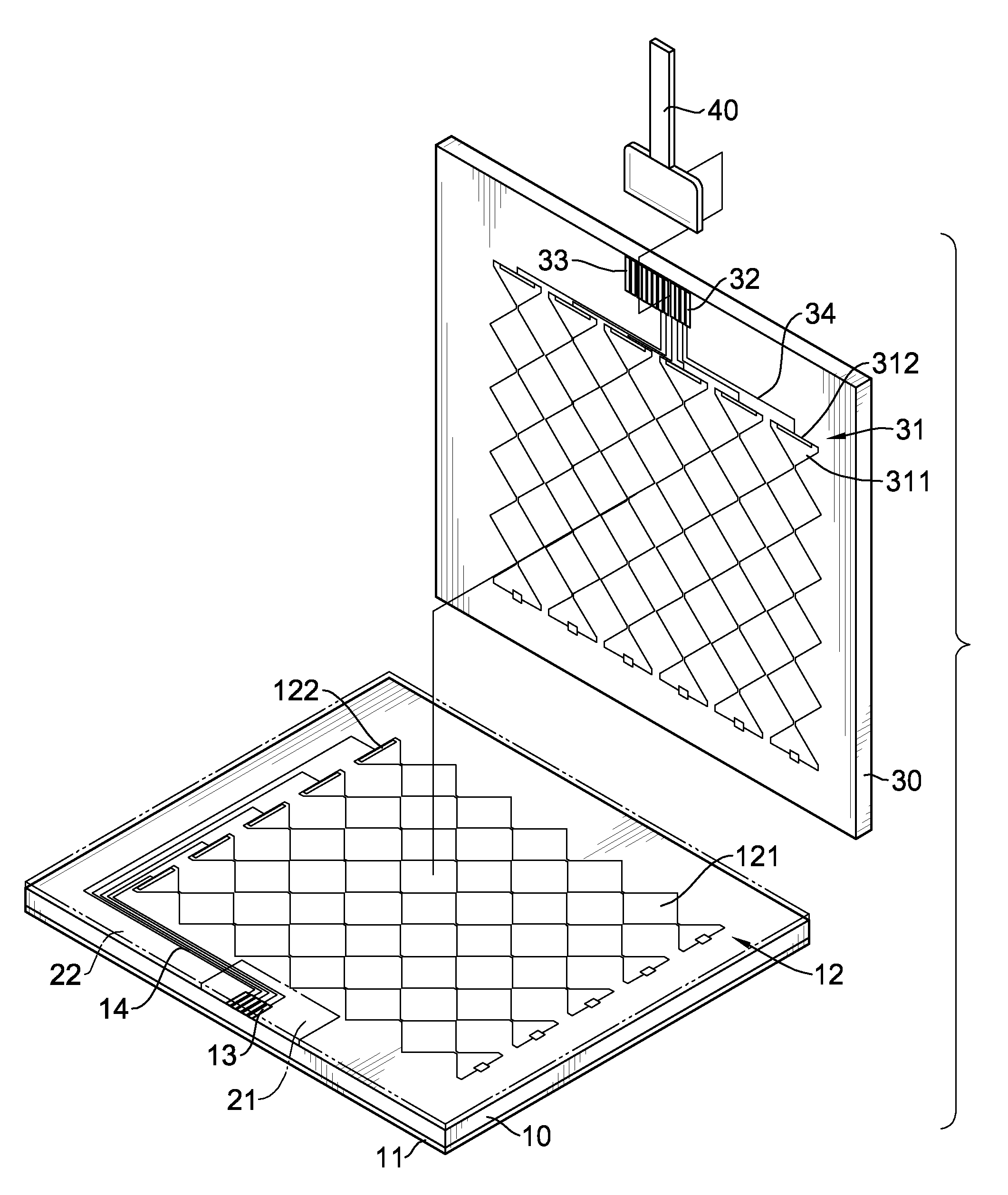
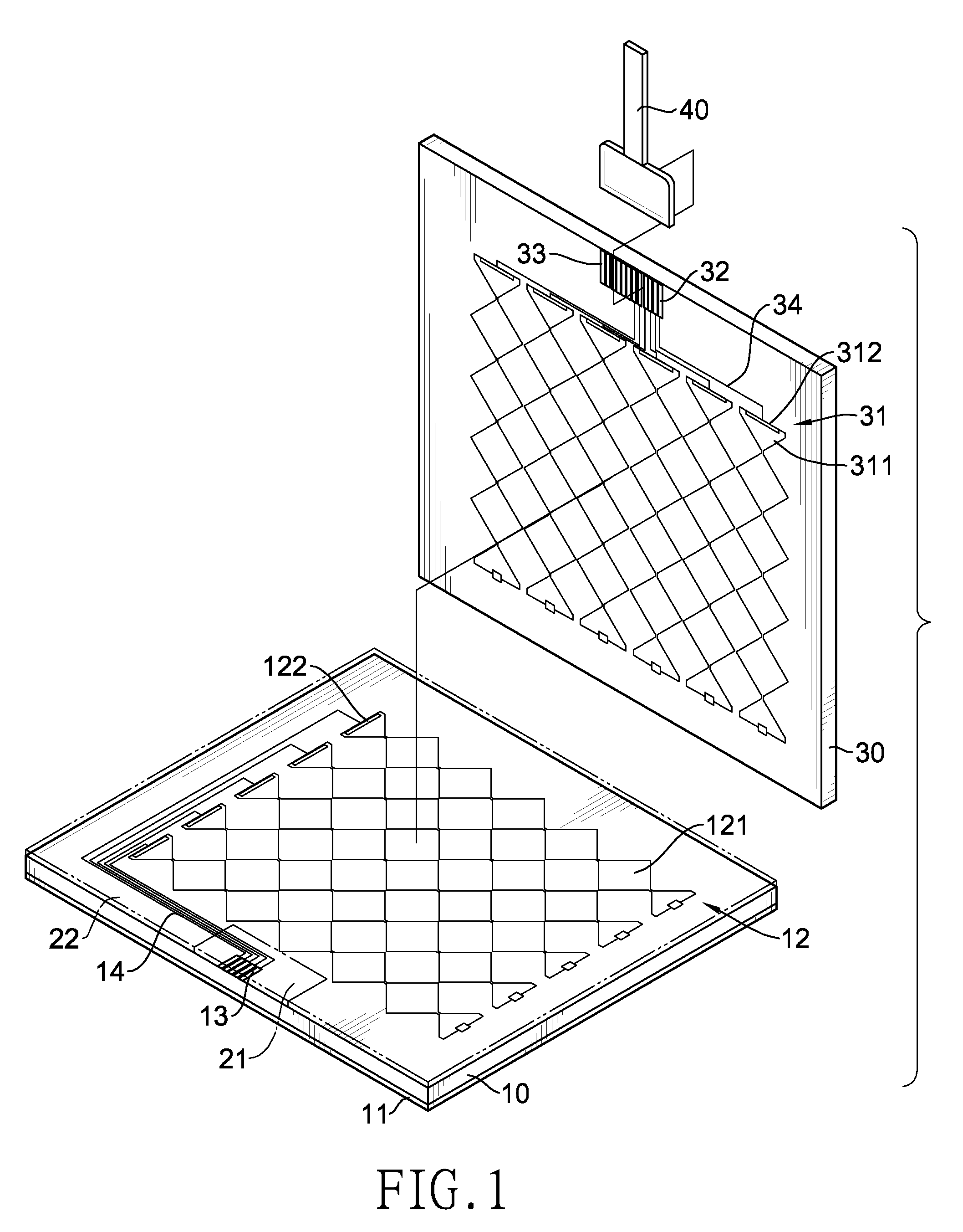
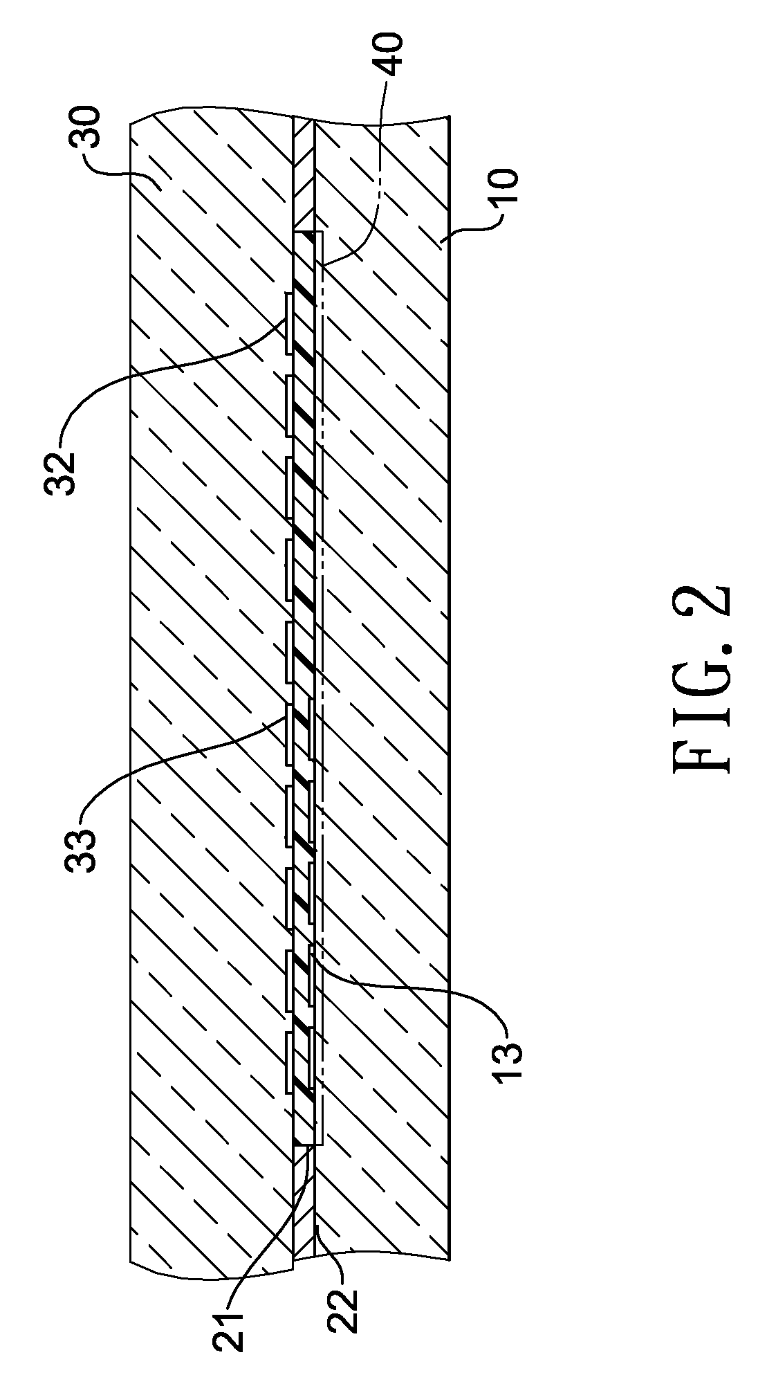
[0031]The present invention can be applied to either a capacitive touch panel or a resistive touch panel. With reference to FIGS. 1 to 3, a capacitive touch panel has a bottom panel 10, an anisotropic conductive film 21, an insulating layer 22, a top panel 30 and a flexible PCB 40.

[0032]The bottom panel 10 has an EMI (electromagnetic interference) shielding layer 11, multiple lower sensing areas 12, multiple first lower ports 122, multiple second lower ports 13 and multiple lower wires 14. The EMI shielding layer 11 is formed on a bottom surface of the bottom panel 10 and is composed of ITO. The lower sensing areas 12 are formed on a top surface of the bottom panel 10, parallelly align in a first direction, and each of the lower sensing areas 12 has multiple lower sensing units 121 serially connected and composed of ITO. Each of the first lower ports 122 is formed on an edge of one of the outermost lower sensing units 121 in the first direction, and is formed by a conductive materia...


PUM


Abstract

A touch panel is characterized in that one side of a top panel protrudes beyond a side of a bottom panel, signals of sensing areas or conductive layer on the top panel for sensing capacitive variation or voltage variation are transmitted to a bottom surface of the protruded side, signals of sensing areas or conductive layer on the bottom panel for sensing capacitive variation or voltage variation are transmitted to a bottom surface of the top panel through conductive adhesives and to the bottom surface of the protruded side, and the top panel has a flexible PCB formed on the bottom surface of the protruded side to receive those signals. As the flexible PCB is not sandwiched between the top and bottom panels, all layers of the touch panel can be uniformly and tightly bonded and touch insensitivity caused by air penetration into the touch panel can be prevented.

Description

BACKGROUND OF THE INVENTION[0001]1. Field of the Invention[0002]The present invention relates to a touch panel, and more particularly to a touch panel with a relatively higher yield and a uniform thickness.[0003]2. Description of the Related Art[0004]Touch panels can be classified as capacitive touch panels, resistive touch panels, surface acoustic touch panels, infrared touch panels and the like in terms of touch panel technologies. Among them, the capacitive touch panels and the resistive touch panels take the leading position in market share. The technologies behind the capactive touch panels and the resistive touch panels determine the location of a touched point based on capactive and voltage variation generated at the touched point. Structurally, both touch panels commonly have an upper substrate and a lower substrate. The surfaces of the upper substrate and the lower substrate that face each other have an indium tin oxide (ITO) layer respectively formed on the surfaces to sen...

Claims


Application Information

Patent Timeline
Patent Type & Authority Patents(United States)
IPC IPC(8): H05K9/00
CPCG06F3/044G06F3/045G06F3/041H05K3/361G06F2203/04107G06F3/0445G06F3/0446
Inventor HSU, JANE
Owner MINLEAD
Why Eureka
Try Eureka