
CMOS image sensor

a cmos image sensor and metal oxide technology, applied in the field of semiconductor technology, can solve the problems of reducing the sensitivity of the cmos image sensor, unable to express dark images, and difficulty in ensuring a sufficient dynamic range, so as to achieve the effect of expanding the dynamic range, avoiding sensitivity loss, and reducing the sensitivity

Active Publication Date: 2013-01-01
SAMSUNG ELECTRONICS CO LTD +1
View PDF12 Cites 8 Cited by
  • Summary
  • Abstract
  • Description
  • Claims
  • Application Information

AI Technical Summary

Benefits of technology

[0019]An object of the present invention is to provide a CMOS image sensor, in which a plurality of floating diffusion regions are provided in a pixel, having the advantage of obtaining an expanded dynamic range without sacrificing sensitivity.
[0021]According to the embodiments of the present invention, a plurality of floating diffusion regions are provided in a pixel to have different capacitance, and thus an expanded dynamic range can be obtained without sacrificing sensitivity.
[0022]According to the embodiments of the present invention, the floating diffusion regions are separated from each other. Therefore, at low illuminance, a vivid image can be obtained with high sensitivity. In addition, at high illuminance, a vivid image can be obtained without causing an image to be saturated and whitened.

Problems solved by technology

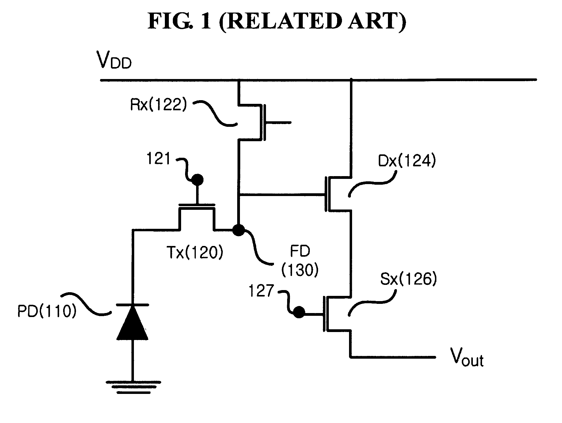
In addition, as a digital camera or a camera-equipped cellular phone is reduced in size, low-voltage driving is performed due to demands for reducing a unit area in the pixels of the image sensor and realizing low power consumption, which makes it difficult to ensure a sufficient dynamic range.
However, if the capacitance is increased, sensitivity of the CMOS image sensor is decreased, and a dark image may not be expressed.

Method used


Image

  • CMOS image sensor
  • CMOS image sensor
  • CMOS image sensor

Examples


Embodiment Construction

[0030]Advantages and features of the present invention and methods of accomplishing the same may be understood more readily by reference to the following detailed description of preferred embodiments and the accompanying drawings. The present invention may, however, be embodied in many different forms and should not be construed as being limited to the embodiments set forth herein. Rather, these embodiments are provided so that this disclosure will be thorough and complete and will fully convey the concept of the present invention to those skilled in the art, and the present invention will only be defined by the appended claims.

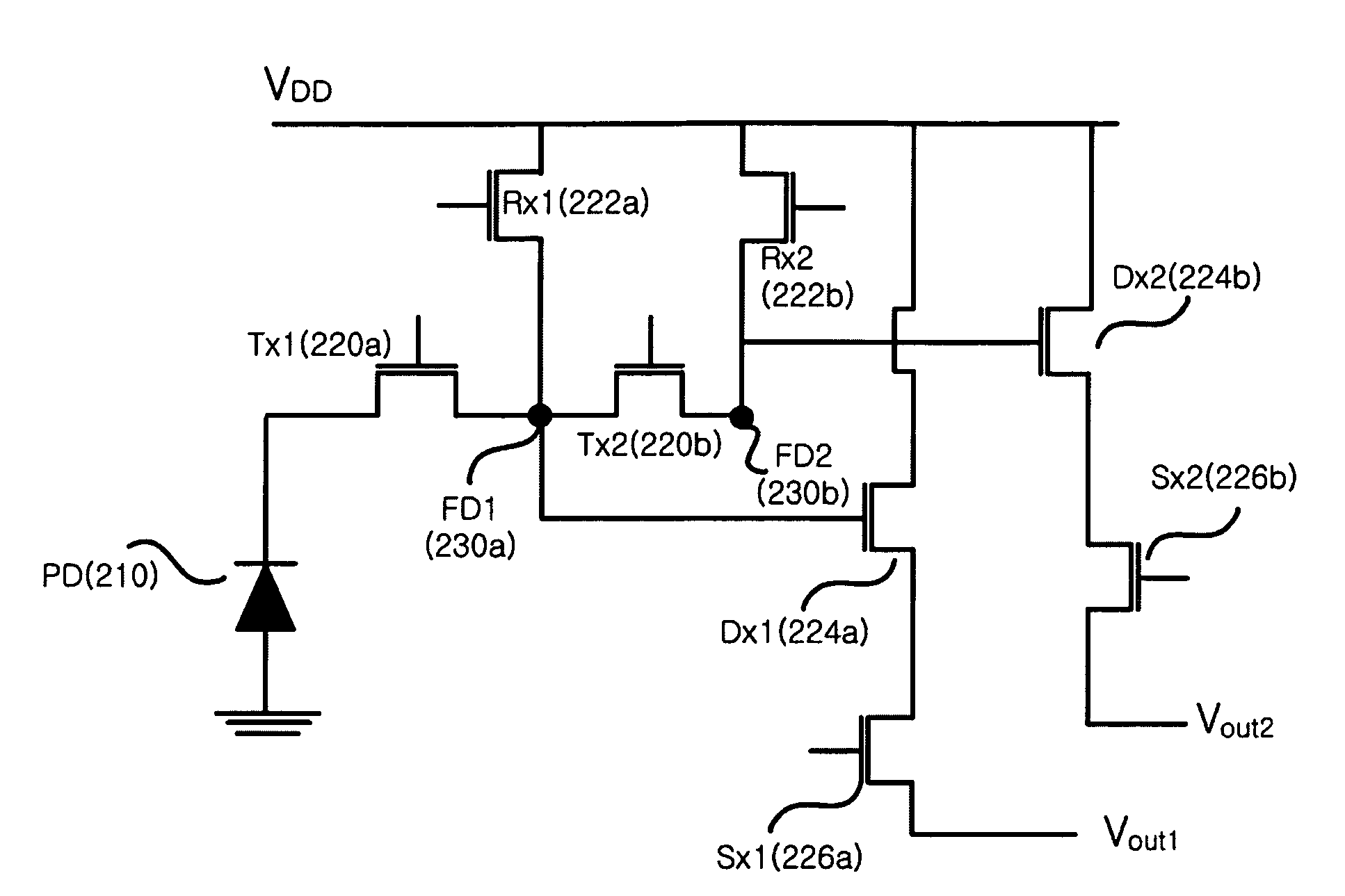
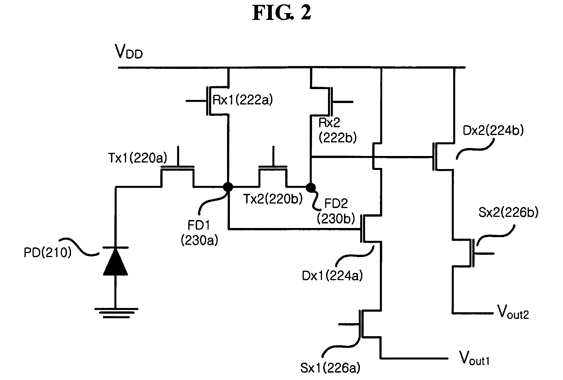
[0031]FIG. 2 is a circuit diagram showing a unit pixel of a CMOS image sensor having two floating diffusion regions according to an embodiment of the present invention.

[0032]Referring to FIG. 2, a CMOS image sensor according to an embodiment of the present invention has a first floating diffusion region (FD1) 230a and a second floating diffusion region (FD2) ...


PUM


Abstract

A CMOS (Complementary Metal-Oxide Semiconductor) image sensor is provided. A CMOS image sensor includes a first light-receiving unit converting light into charge, a first floating diffusion region, in which a first potential corresponding to the converted amount of charge is generated and a second floating diffusion region, to which the charge in the first floating diffusion region is transmitted, and in which a second potential is generated, wherein a wide dynamic range signal is acquired from the first floating diffusion region, a high-sensitively signal is acquired from the second floating diffusion region, and the acquired signals are synthesized and output.

Description

CROSS REFERENCE TO RELATED APPLICATION[0001]This application claims priority from Korean Patent Application No. 10-2007-0077016 filed on Jul. 31, 2007 in the Korean Intellectual Property Office, the disclosure of which is incorporated herein by reference in its entirety.BACKGROUND OF THE INVENTION[0002]1. Field of the Invention[0003]The present invention relates to a semiconductor technology, and, in particular, to a CMOS (Complementary Metal-Oxide Semiconductor) image sensor that has an expanded dynamic range.[0004]2. Description of the Related Art[0005]In recent years, high-resolution camera-equipped apparatuses, such as digital cameras, camera-equipped cellular phones, and surveillance cameras, have become widespread. As an imaging device for such a camera, a CCD (Charge Coupled Device) or a CMOS (Complementary Metal-Oxide Semiconductor) image sensor is used.[0006]The CMOS image sensor has features of ease of manufacturing and low cost compared with the CCD, and thus it is popula...

Claims


Application Information

Patent Timeline
Patent Type & Authority Patents(United States)
IPC IPC(8): H04N5/335
CPCH01L27/14609H04N5/3559H04N3/155H04N5/35545H04N5/35563H01L27/14603H01L27/14643H01L31/035281H04N25/581H04N25/585H04N25/59H04N25/771H01L27/146
Inventor SONG, HYUN-CHULLEE, SEONG-DEOKCHOE, WON-HEEKWON, JAE-HYUNLEE, KANG-EUI
Owner SAMSUNG ELECTRONICS CO LTD
Learn More