Stacked piezoelectric device

a piezoelectric device and piezoelectric technology, applied in the direction of generators/motors, mechanical equipment, machines/engines, etc., can solve the problems of sacrificing the amount of displacement, concentrating stress at the interface, and cracks in the device, so as to avoid the drop in insulation resistance.

Active Publication Date: 2012-08-14
DENSO CORP
View PDF34 Cites 0 Cited by
  • Summary
  • Abstract
  • Description
  • Claims
  • Application Information

AI Technical Summary

Benefits of technology

[0021]Generally, when high electric field continues to be applied to the stacked piezoelectric device at high temperature, the phenomenon that a lower resistance area spreads from the negative electrode side will appear. For example, the cause is that when the stacked piezoelectric device is made integrally by the firing, conductive metallic ions, as spreading to the piezoelectric ceramic layers during the firing, are metalized by electrons emitted from the negative electrode. The above phenomenon results in a variation in distribution of electric field intensity oriented in the laminating direction between the positive electrode layer and the negative electrode layer. In other words, the electric field intensity drops in the low resistance area, thereby resulting in a rise in electric field intensity in areas other than the low resistance area. The rise in electric field intensity accelerates the deterioration of the insulation resistance. The spreading of the low resistance area is usually accelerated by the existence of water.
[0027]Consequently, the piezoelectric ceramic layers including the stress absorbing portion are used as driving layers, but application of an excessive electric field to the stress absorbing portions is controlled or avoided. It is, therefore, possible to avoid the drop in insulation resistance without almost sacrificing the amount of displacement.
[0036]In the above second invention, there is no portion which most accelerates the drop in insulation resistance, that is, a portion where the stress absorbing portion to which a great voltage is to be applied overlaps the above described piezoelectric layer driving area end in the laminating direction. This enables the piezoelectric ceramic layer including the stress absorbing portion to be used as a drive source and also reduces the electric field to be applied to the portion susceptible to the drop in insulation resistance, thus avoiding the drop in insulation resistance and providing the stacked piezoelectric device which is excellent in durability.
[0042]Therefore, the piezoelectric ceramic layer including the stress absorbing portion is used as a drive source, but application of an excessive electric field to the stress absorbing portions is controlled or avoided. It is, therefore, possible to avoid the drop in insulation resistance without almost sacrificing the amount of displacement.

Problems solved by technology

However, the formation of the inner electrode-unformed areas in order to improve the insulation may cause portions which are susceptible and insusceptible to deformation to appear in the ceramic laminate upon application of voltage thereto, resulting in concentration of stress at interfaces therebetween and cracks in the device.
However, even when the stress absorbing portions are formed, the application of the voltage to the stress absorbing portions also may result in cracks extending from the top end of the stress absorbing portions.
Such a structure, however, causes great electric discharge to occur at the stress absorbing portions (grooves) upon application of great voltage thereto, so that they may be short-circuited.
This gives rise to the problem of insufficient electric insulation, which results in a decrease in service life of the stacked piezoelectric devices.
However, in fact, even when no cracks occur in the stress absorbing portions, it is still difficult to ensure sufficient electric insulation, which gives rise to the problem of a drop in electric insulation, thus resulting in formation of cracks.
This results in the problem of a decreased amount of stroke of the stacked piezoelectric devices.

Method used


Image

  • Stacked piezoelectric device
  • Stacked piezoelectric device
  • Stacked piezoelectric device

Examples


embodiments

[0172](Embodiment 1)

[0173]Next, the stacked piezoelectric device according to embodiments of the invention will be described below using FIGS. 1 to 10.

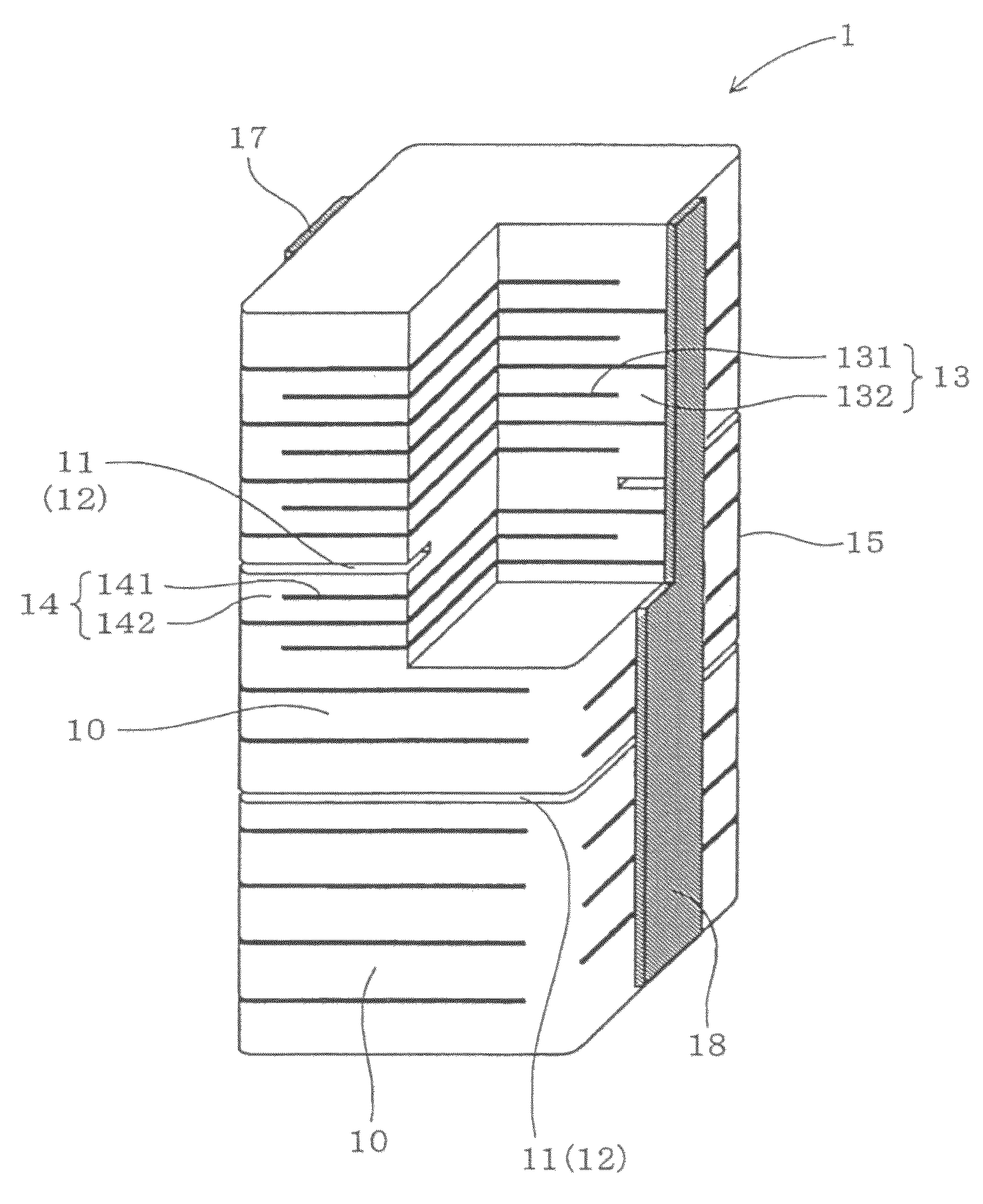
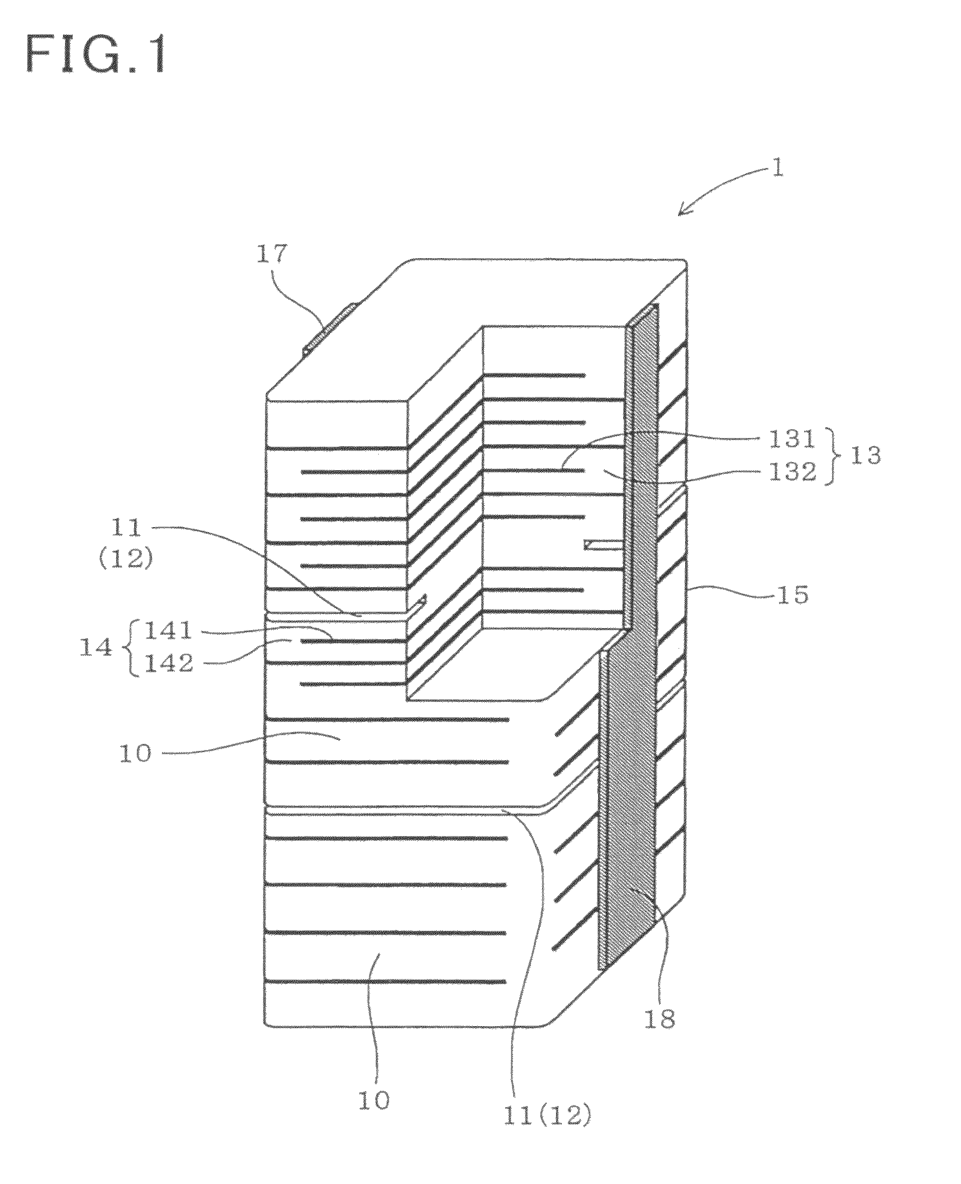
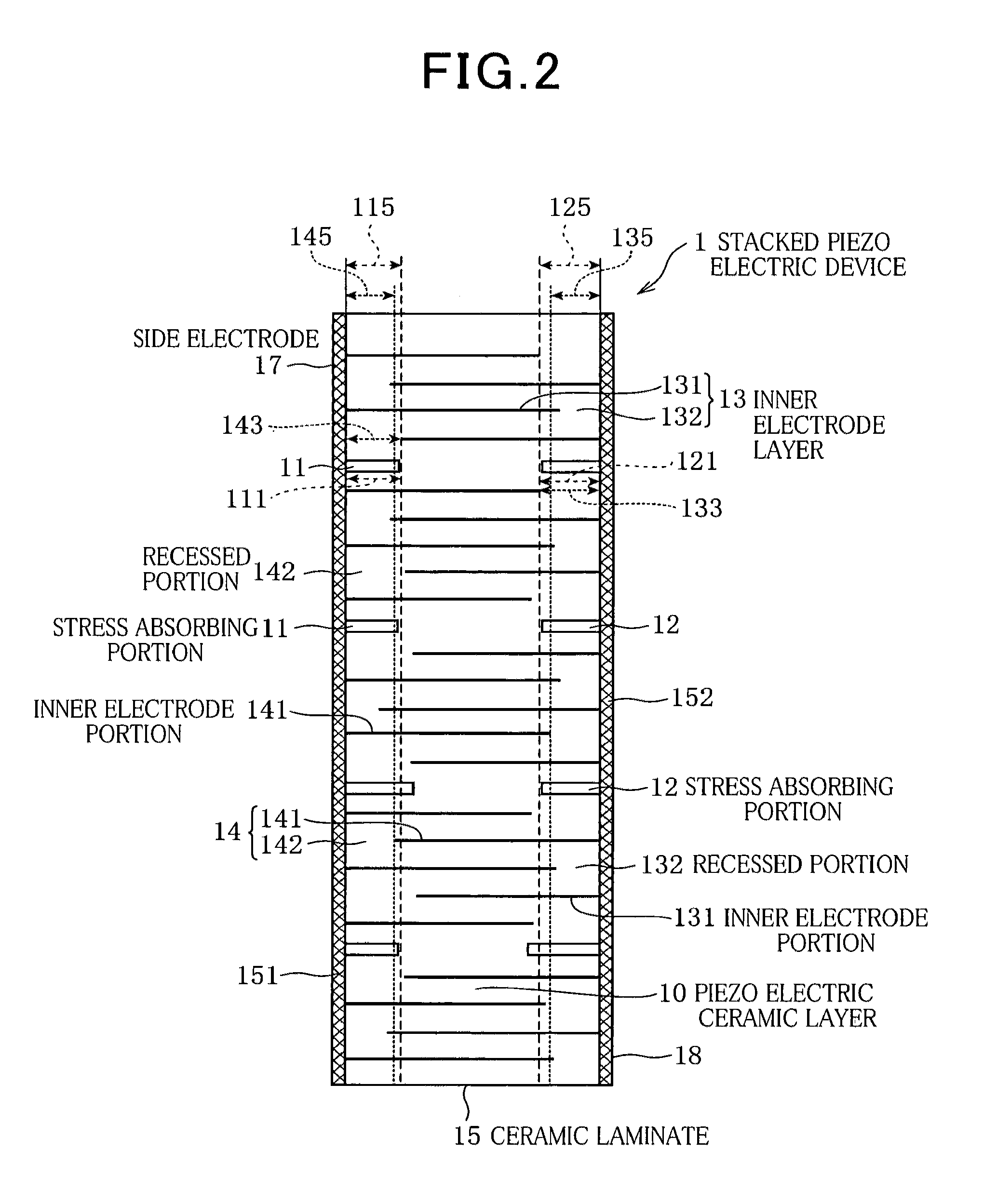
[0174]As illustrated in FIGS. 1 to 3, the stacked piezoelectric device 1 of this embodiment has a ceramic laminate 15 made by stacking the plurality of piezoelectric layers 10 and the plurality of inner electrode layers 13 and 14 alternately and the pair of side electrodes 17 and 18 fanned on side surfaces of the ceramic laminate 15. The inner electrode layers 13 and 14 include the conductive inner electrode portions 131 and 141 and the recessed portions 132 and 142 defined by retreating outer peripheral ends of the inner electrode portions 131 and 141 inwardly from the outer peripheral surface of the ceramic laminate 15. The inner electrode layers 13 and 14 are connected electrically to side electrodes 17 and 18, respectively, which are different from each other. Specifically, the inner electrode layers 13 and 14 are equipped with th...


PUM

PropertyMeasurementUnit
depthaaaaaaaaaa
depthaaaaaaaaaa
depthsaaaaaaaaaa

Abstract

A stacked piezoelectric device 1 including a ceramic laminate formed by laminating piezoelectric ceramic layers and inner electrode layers alternately and a pair of side electrodes. The inner electrode layers 13 and 14 have inner electrode portions 131 and 141 and the recessed portions 132 and 142. The ceramic laminate 15 has the stress absorbing portions 11 and 12. A recessed distance of one of two of the recessed portions 132 and 142 which interleave the stress absorbing portions 11 and 12 therebetween which is located on the same side surface as the stress absorbing portion 11 or 12 is greater than the depth of the stress absorbing portion 11 and 12.

Description

This application is the U.S. national phase of International Application No.[0001]PCT / JP2008 / 053229 filed 26 Feb. 2008 which designated the U.S. and claims priority to Japanese Patent Application Nos. 2007-046070 filed 26 Feb. 2007, 2008-017946 filed 29 Jan. 2008 and 2008-042111 filed 22 Feb. 2008, the entire contents of each of which are hereby incorporated by reference.TECHNICAL FIELD[0002]The present invention relates to a stacked piezoelectric device equipped with a ceramic laminate made up of a plurality of piezoelectric ceramic layers and a plurality of inner electrode layers which are laminated alternately, a pair of side electrodes formed on side surfaces of the ceramic layer laminate, and stress absorbing portions formed in slit-like areas depressed inwardly into the sides of the ceramic laminate.BACKGROUND ART[0003]Conventionally, stacked piezoelectric devices are used as drive source of fuel injectors. The stacked piezoelectric device is made up of, for example, a ceramic...

Claims


Application Information

Patent Timeline
Patent Type & Authority Patents(United States)
IPC IPC(8): B05B1/08H01L41/083H01L41/187H01L41/22H01L41/27H01L41/293H01L41/297H01L41/39
CPCH01L41/0838H01L41/273F02M63/0026H10N30/508H10N30/053
Inventor SUZUKI, SATOSHIMURAI, ATSUSHIASANO, HIROAKINODA, KOUJINAGAYA, TOSHIATUIWASE, AKIOFUJII, AKIRAKADOTANI, SHIGE
Owner DENSO CORP
Why Eureka
Try Eureka