Semiconductor device including increased capacity leadframe

a semiconductor and leadframe technology, applied in semiconductor devices, semiconductor/solid-state device details, electrical apparatus, etc., can solve the problems of increasing the overall size of the qfp package, further limiting the number of inputs/outputs (i/o's), and conventional leadframe structures as currently known and integrated into existing qfp packages often prove unsatisfactory, so as to achieve the effect of effectively electrically isolating various leads within the semiconductor packag

Active Publication Date: 2012-01-03
AMKOR TECH SINGAPORE HLDG PTE LTD
View PDF451 Cites 16 Cited by
  • Summary
  • Abstract
  • Description
  • Claims
  • Application Information

AI Technical Summary

Benefits of technology

[0013]In accordance with the present invention, there is provided a semiconductor package (e.g., a QFP package) including a uniquely configured leadframe sized and configured to maximize the available number of exposed leads in the semiconductor package. More particularly, the semiconductor package of the present invention includes a generally planar die pad or die paddle defining multiple peripheral edge segments. In addition, the semiconductor package includes a plurality of leads. Some of these leads are provided in two concentric rows or rings which at least partially circumvent the die pad, with other leads including portions which protrude from respective side surfaces of a package body of the semiconductor package. Connected to the top surface of the die pad is at least one semiconductor die which is electrically connected to at least some of the leads. At least portions of the die pad, the leads, and the semiconductor die are encapsulated by the package body. In one embodiment of the present invention, those leads which do not protrude from a side surface of the package body are aligned with respective ones of a plurality of vias or openings which are formed in the package body and filled with a conductive metal material. In another embodiment of the present invention, at least portions of the bottom surfaces of the die pad and those leads which do not protrude from a side surface of the package body are exposed in a common exterior surface of the package body. The leadframe of the semiconductor package is fabricated in accordance with standard, low-cost forming techniques. In accordance with the present invention, sawing, punching, etching, or other material removal processes may be completed during the fabrication of the semiconductor package to effectively electrically isolate various leads from each other within the semiconductor package. The semiconductor package of the present invention may include one or more internal semiconductor dies, depending on functional requirements.

Problems solved by technology

One of the size deficiencies of currently known QFP packages is attributable to the length at which the leads protrude from the sides of the package body, such protrusion length resulting in an increase in the overall size of the QFP package and further limiting the number of inputs / outputs (I / O's) which may be included therein.
In view of this need, conventional leadframe structures as currently known and integrated into existing QFP packages often prove to be unsatisfactory.
However, the circuit boards integrated into these types of semiconductor packages are expensive and typically exhibit poor heat sink and electrical performance characteristics in comparison to semiconductor packages employing leadframes.
Such a structure is difficult to achieve in a semiconductor package employing a circuit board.
Additionally, though certain BGA semiconductor packages include metal leadframes, the process of bending the leadframe to create the lands upon which the solder balls are ultimately formed often deforms the leadframe in a manner creating imperfect wiring bonding areas for the semiconductor die.
These imperfections could potentially give rise to undesirable occurrences of stitch bond lift, wire shorting and / or sagging, mold void (imperfect molded state at the edges of a land), and mold flash (a state where resin smear remains on the exposed surface of a land).

Method used


Image

  • Semiconductor device including increased capacity leadframe
  • Semiconductor device including increased capacity leadframe
  • Semiconductor device including increased capacity leadframe

Examples


first embodiment

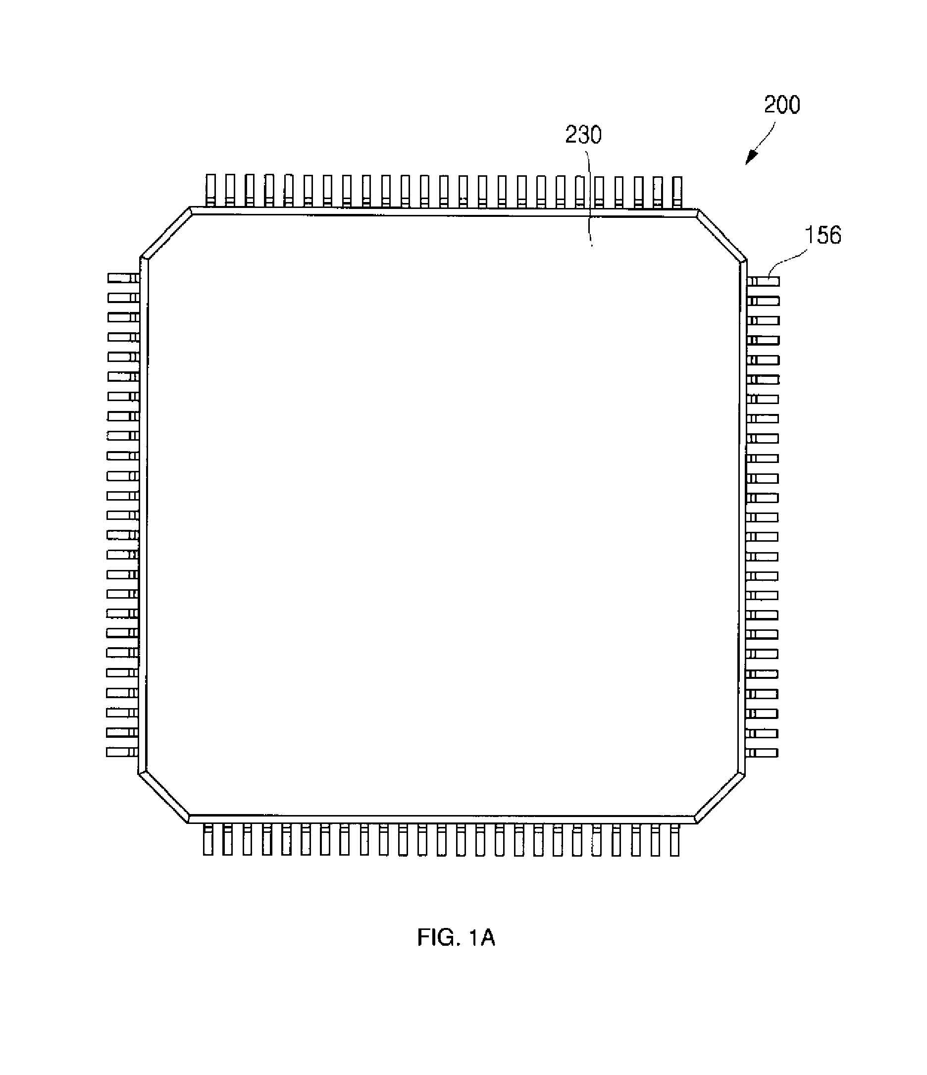
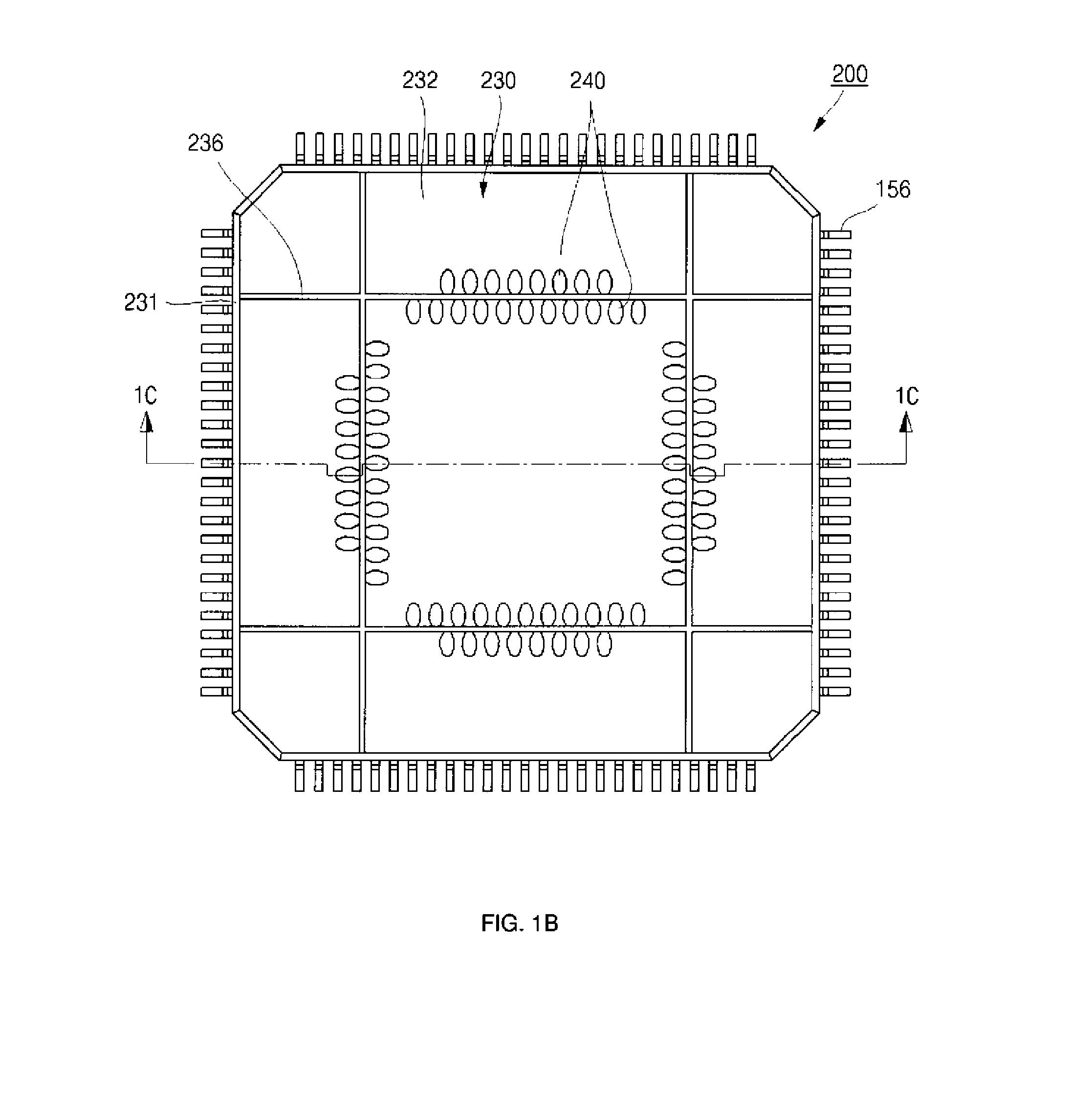
[0029]Referring now to the drawings wherein the showings are for purposes of illustrating one embodiment of the present invention only, and not for purposes of limiting the same, FIG. 1D depicts a leadframe 100 for integration into a semiconductor package 200 constructed in accordance with the present invention. The semiconductor package 200 is shown in FIGS. 1A, 1B and 1C.

[0030]Referring now to FIG. 1D, the leadframe 100 of the present invention comprises a generally quadrangular (e.g., square) die pad 110 which defines four peripheral edge segments and opposed, generally planar top and bottom surfaces. Integrally connected to the die pad 110 is a plurality of tie bars 120. More particularly, the leadframe 100 includes four tie bars 120 which extend diagonally from respective ones of the four corner regions defined by the die pad 110. Each of the tie bars 120 defines opposed, generally planar top and bottom surfaces which extend in generally coplanar relation to respective ones of ...

second embodiment

[0058]Referring now to FIG. 2, there is shown a semiconductor package 400 constructed in accordance with the present invention. The semiconductor package 400 is similar in structure to the semiconductor package 200 described above, with only the differences between the semiconductor packages 400, 200 being described below.

[0059]The semiconductor package 400 includes the same leadframe 100 described above in relation to the semiconductor package 200. Additionally, the semiconductor package 400 also includes the semiconductor die 210 and the conductive wires 220 which are mechanically and electrically connected to the leadframe 100 in the same manner described above in relation to the semiconductor package 200. Thus, the sole distinction between the semiconductor packages 400, 200 lies in the structural attributes of the package body 430 of the semiconductor package 400 in comparison to the package body 230 of the semiconductor package 200.

[0060]More particularly, during the fabricati...

third embodiment

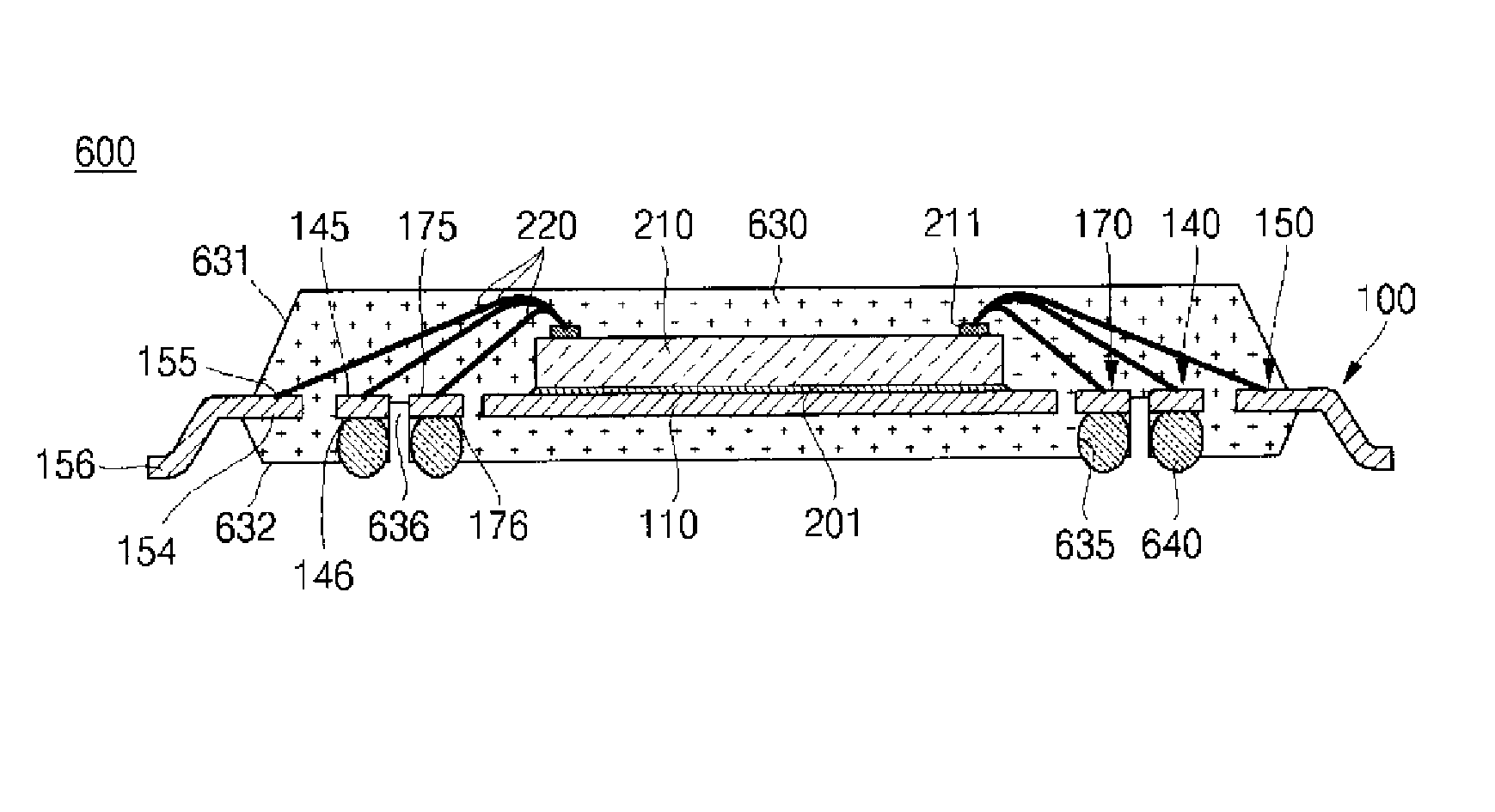
[0069]Referring now to FIG. 3, there is shown a semiconductor package 600 constructed in accordance with the present invention. The semiconductor package 600 is similar in structure to the semiconductor package 200 described above, with only the differences between the semiconductor packages 600, 200 being described below.

[0070]The semiconductor package 600 includes the same leadframe 100 described above in relation to the semiconductor package 200. Additionally, the semiconductor package 600 also includes the semiconductor die 210 and the conductive wires 220 which are mechanically and electrically connected to the leadframe 100 in the same manner described above in relation to the semiconductor package 200. Thus, the sole distinction between the semiconductor packages 600, 200 lies in the structural attributes of the package body 630 of the semiconductor package 600 in comparison to the package body 230 of the semiconductor package 200.

[0071]More particularly, during the fabricati...


PUM


Abstract

In accordance with the present invention, there is provided a semiconductor package (e.g., a QFP package) including a uniquely configured leadframe sized and configured to maximize the available number of exposed leads in the semiconductor package. More particularly, the semiconductor package of the present invention includes a generally planar die pad or die paddle defining multiple peripheral edge segments. In addition, the semiconductor package includes a plurality of leads. Some of these leads are provided in two concentric rows or rings which at least partially circumvent the die pad, with other leads including portions which protrude from respective side surfaces of a package body of the semiconductor package. Connected to the top surface of the die pad is at least one semiconductor die which is electrically connected to at least some of the leads. At least portions of the die pad, the leads, and the semiconductor die are encapsulated by the package body.

Description

CROSS-REFERENCE TO RELATED APPLICATIONS[0001]Not ApplicableSTATEMENT RE: FEDERALLY SPONSORED RESEARCH / DEVELOPMENT[0002]Not ApplicableBACKGROUND OF THE INVENTION[0003]1. Field of the Invention[0004]The present invention relates generally to integrated circuit package technology and, more particularly, to an increased capacity QFP semiconductor package which includes exposed leads and an exposed die pad on the bottom surface of the package body thereof, and additional leads which protrude from side surfaces of the package body.[0005]2. Description of the Related Art[0006]Semiconductor dies are conventionally enclosed in plastic packages that provide protection from hostile environments and enable electrical interconnection between the semiconductor die and an underlying substrate such as a printed circuit board (PCB) or motherboard. The elements of such a package include a metal leadframe, an integrated circuit or semiconductor die, bonding material to attach the semiconductor die to ...

Claims


Application Information

Patent Timeline
Patent Type & Authority Patents(United States)
IPC IPC(8): H01L23/48H01L23/02H01L29/40H01L23/495H01L23/52H01L23/28
CPCH01L21/4842H01L23/3107H01L23/49517H01L23/49541H01L24/29H01L24/45H01L24/48H01L24/83H01L24/85H01L2224/2919H01L2224/45124H01L2224/45139H01L2224/45144H01L2224/45147H01L2224/48091H01L2224/48247H01L2224/49171H01L2224/73265H01L2224/83101H01L2224/85H01L2224/92H01L2224/92247H01L2924/01015H01L2924/0105H01L2924/01078H01L2924/01079H01L2924/078H01L2924/15311H01L2924/1815H01L2924/00014H01L2924/0665H01L24/49H01L2224/32245H01L2924/00012H01L2924/01013H01L2924/01028H01L2924/00H01L2924/01047H01L24/73H01L2924/14H01L2924/181H01L2224/05554H01L2224/45015H01L2924/207
Inventor KIM, GWANG HOKIM, JIN SEONGPARK, DONG JOOKANG, DAE BYOUNG
Owner AMKOR TECH SINGAPORE HLDG PTE LTD
Why Eureka
Try Eureka