Image forming apparatus
a technology of image forming apparatus and forming apparatus, which is applied in the direction of electrographic process apparatus, instruments, optics, etc., can solve the problems of reducing the transfer rate and density of toner in resulting images, and weak transfer field to attract toner particles
- Summary
- Abstract
- Description
- Claims
- Application Information
AI Technical Summary
Benefits of technology
Problems solved by technology
Method used
Image
Examples
experiment 1
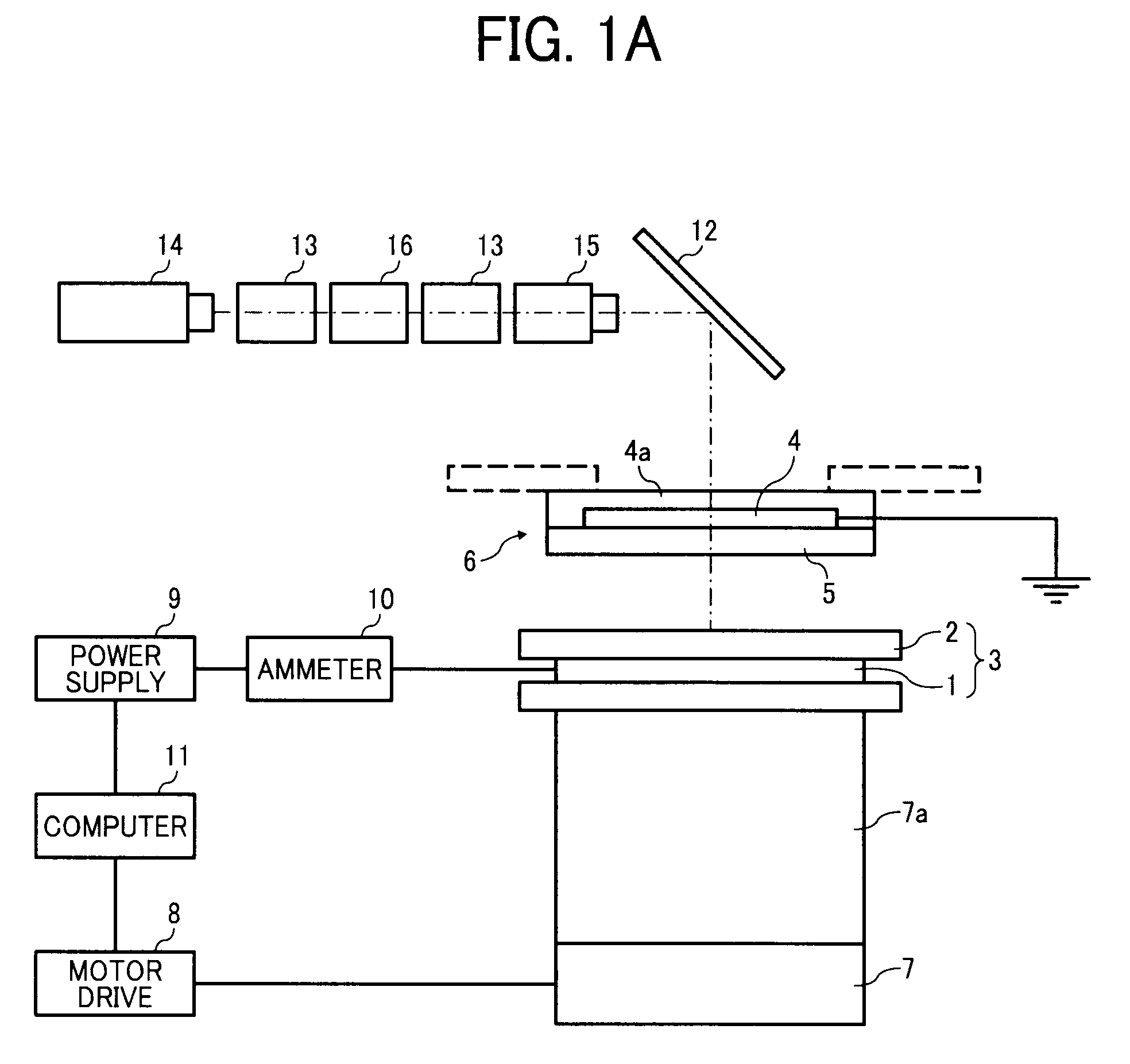
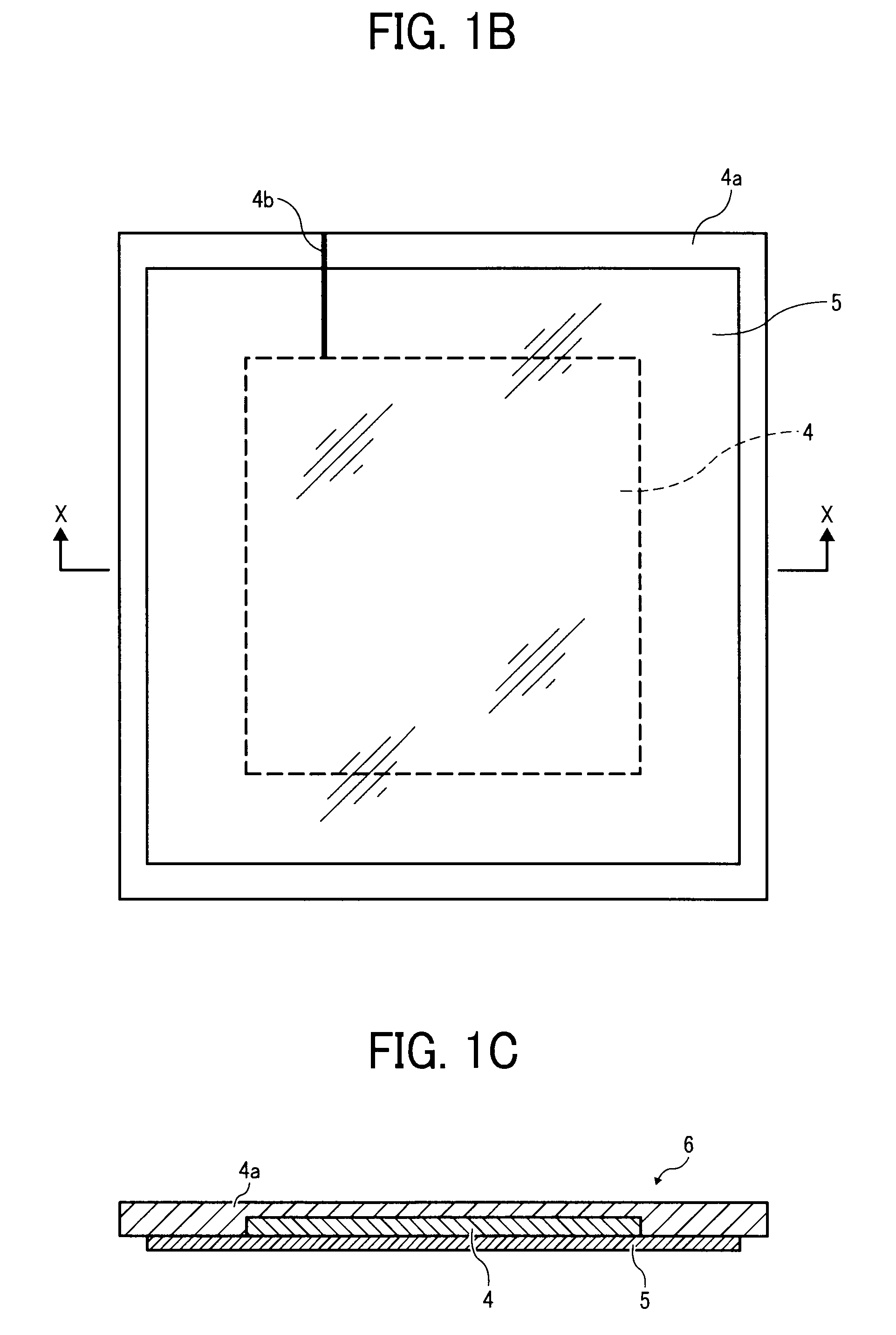
[0046]The ITO substrate 6 bearing a developed toner image thereon was set in place, and the stepper motor 7 moved the SS-PI substrate 3 closer to the ITO substrate 6 while the power supply 9 applied a given constant voltage to the SS electrode 1 so as to transfer toner particles from the PC surface to the PI surface. After transfer, the lower substrate 3 was retracted away from the upper substrate 6, and the weight of toner particles present on the PI sheet 2 was measured.
[0047]The above procedure was repeated using different bias voltages ranging from 0 to 1700 V, for each of which a transfer rate of toner was calculated according to the following equation:
Transfer rate(%)=Wa / Wb*100 Equation 1
[0048]where “Wa” is an amount of toner particles present on the PI surface after transfer, and “Wb” is an amount of toner particles forming an image developed on the PC-ITO substrate prior to transfer.
[0049]FIG. 2 shows results of Experiment 1, plotting calculated transfer rates against appl...
experiment 2
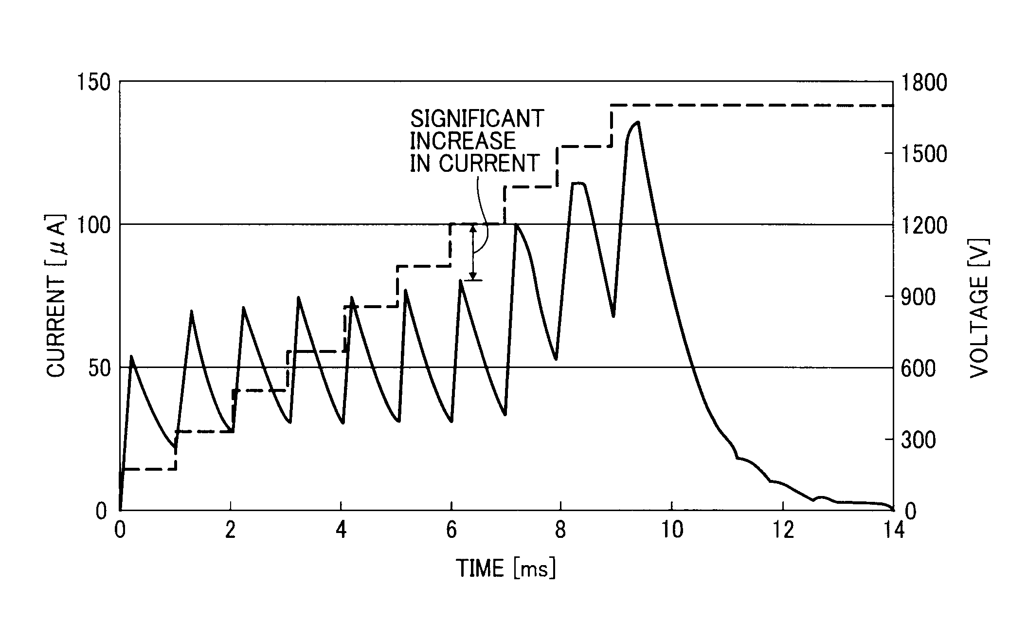
[0052]The ITO substrate 6 bearing a developed toner image thereon was set in place, and the stepper motor 7 moved the SS-PI substrate 3 closer to the ITO substrate 6 while the power supply 9 applied a stepped-up voltage to the SS electrode 1 so as to transfer toner particles from the PC surface to the PI surface. During transfer, the ammeter 10 measured the current flowing into the SS electrode 1 with the bias voltage increased from 170 V to 1700 V in steps of 170 V per millisecond.
[0053]FIG. 3 shows measurement results of Experiment 2, plotting the output current in microamperes (solid line) with the applied bias voltage in volts (dotted line) against time in milliseconds.
[0054]As shown in FIG. 3, the current output to the electrode 1 traces a substantially regular, periodic waveform when the bias voltage is stepped up to 1190 V, except for the first millisecond in which the current level still remains low. The output current significantly increases as the applied voltage increases...
experiment 3
[0110]Printing was performed using plain A4 size copy paper (T6200 A4Y available from Ricoh Company Ltd.) and a direct transfer tandem color printer.
[0111]Initially, development was performed with suitable photoconductor charge and development bias so as to obtain a monochrome solid image with an area of 8 cm2 and a toner density of 0.4 mg / cm2 on the photoconductor drum. The toner image was then transferred to the copy paper by applying a given current bias. After transfer, the print engine was halted, and toner particles remaining on the surface of the photoconductor were collected by suction.
[0112]The above procedure was repeated with various transfer bias currents (5, 10, 20, 30, 40, 50, and 60 μA), for each of which a transfer rate was calculated according to the following equation:
Transfer rate(%)=(Wc−Wd) / Wc*100 Equation 3
[0113]where “Wc” is the weight of toner present on the photoconductor prior to transfer, and “Wd” is the weight of toner remaining on the photoconductor aft...
PUM
 Abstract
Description
Claims
Application Information
 - R&D
- Intellectual Property
- Life Sciences
- Materials
- Tech Scout
- Unparalleled Data Quality
- Higher Quality Content
- 60% Fewer Hallucinations
Browse by: Latest US Patents, China's latest patents, Technical Efficacy Thesaurus, Application Domain, Technology Topic, Popular Technical Reports.
© 2025 PatSnap. All rights reserved.Legal|Privacy policy|Modern Slavery Act Transparency Statement|Sitemap|About US| Contact US: help@patsnap.com


