Contact element for press fitting into a hole of a printed circuit board
- Summary
- Abstract
- Description
- Claims
- Application Information
AI Technical Summary
Benefits of technology
Problems solved by technology
Method used
Image
Examples
Example
DETAILED DESCRIPTION OF THE DRAWINGS
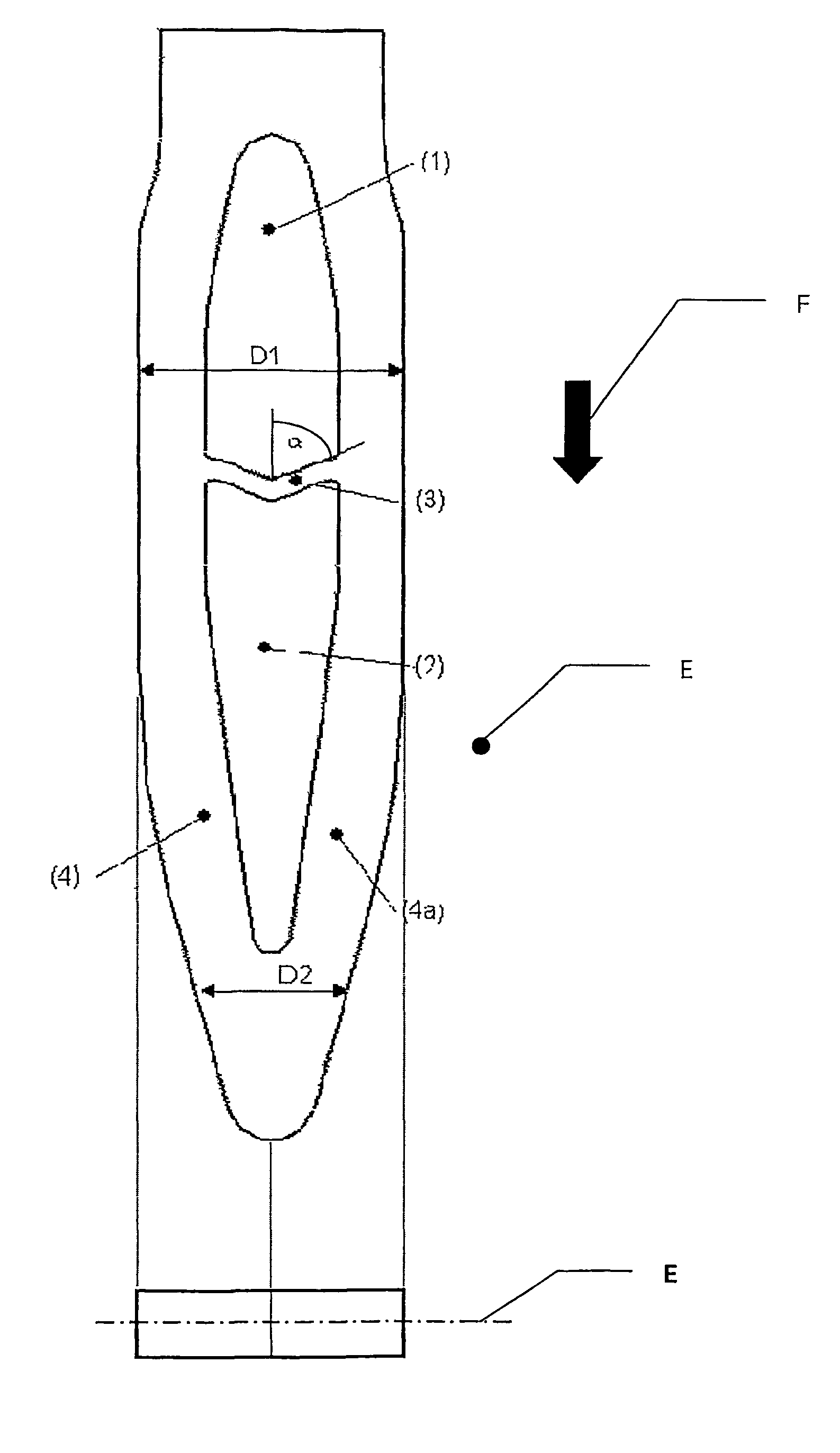
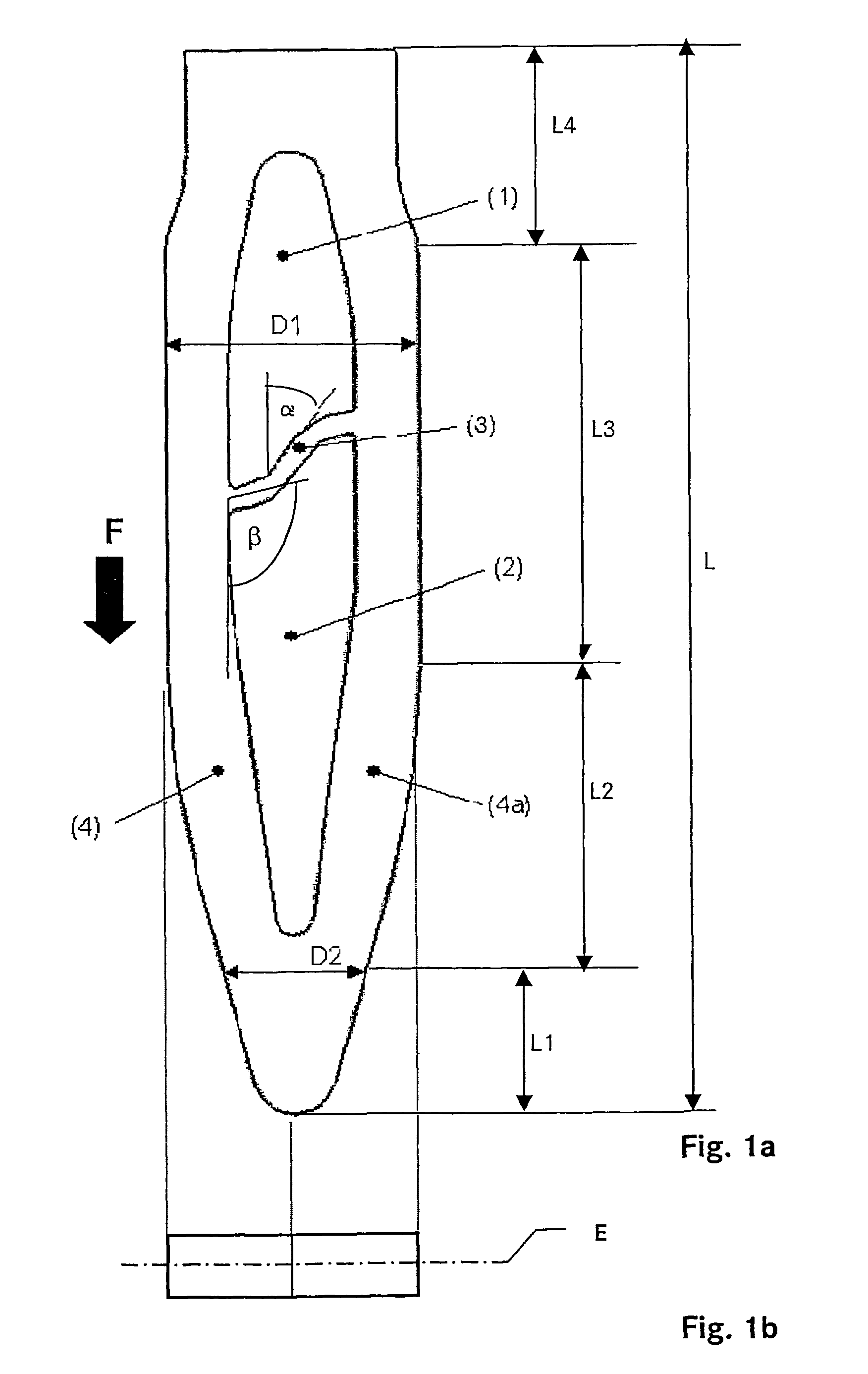
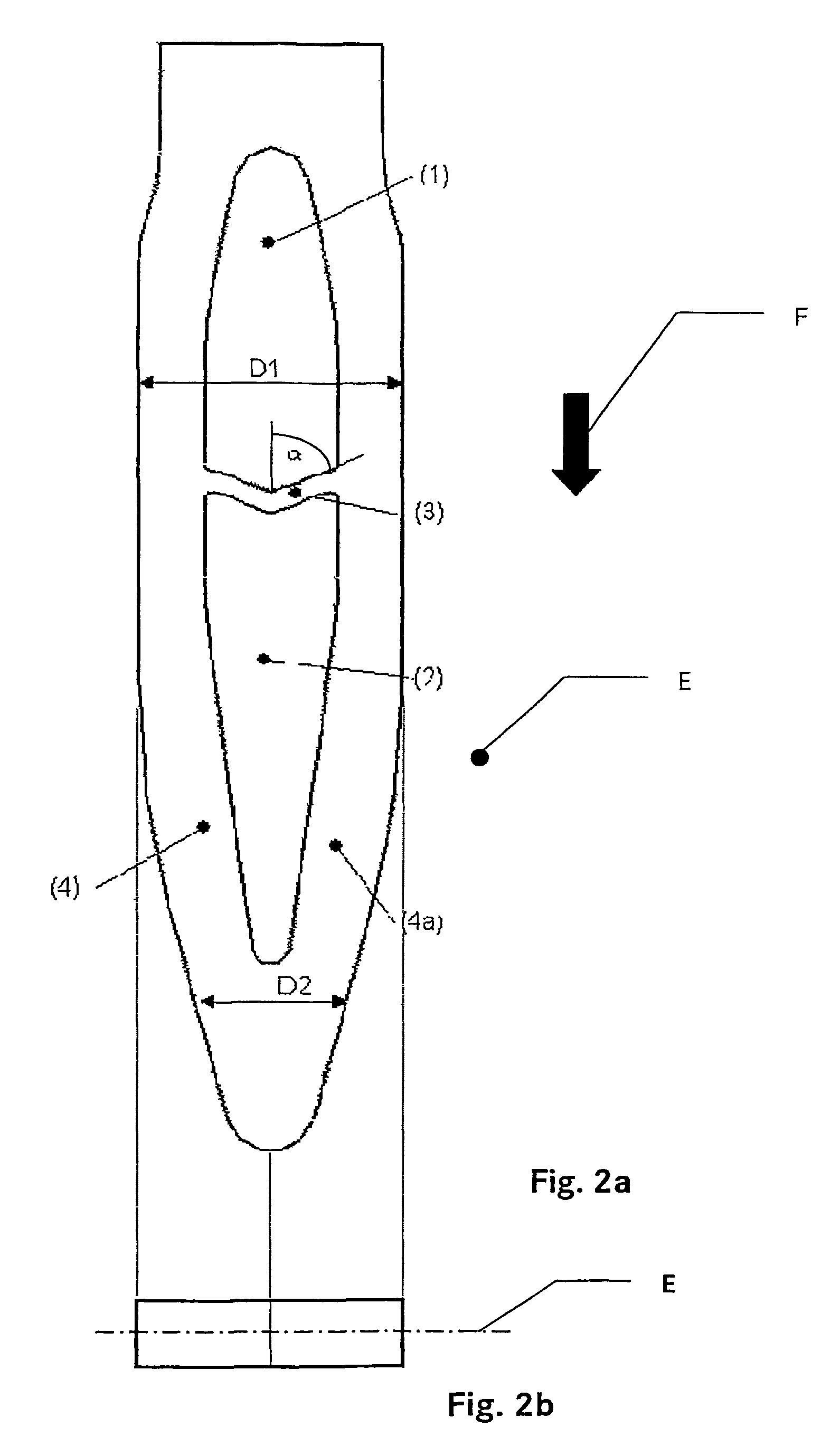
[0019]FIG. 1 shows a contact element for pressing into a hole of a printed circuit board, wherein the contact element comprises a rod-shaped press-fit zone with an insertion region (L1) and an adjacent deformable region (L2, L3).
[0020]The deformable region has a width (D1) which is larger than the diameter of the hole, and the insertion region has a width (D2) which is smaller than the diameter of the hole, so that the contact element can initially be inserted with the insertion region without force being required in the insertion direction F, while aligning itself in the hole due to the angular progress of the limbs in the transfer region L2.
[0021]The deformable region comprises a front (1) and a rear region (2), both of which having a closed opening, which are separated by a crossbar (3). The limbs (4, 4a) are thus separated in the deformable region by an elongated hole, which is subdivided into two openings by a crossbar which connects the limb...
PUM
 Abstract
Description
Claims
Application Information
 - R&D
- Intellectual Property
- Life Sciences
- Materials
- Tech Scout
- Unparalleled Data Quality
- Higher Quality Content
- 60% Fewer Hallucinations
Browse by: Latest US Patents, China's latest patents, Technical Efficacy Thesaurus, Application Domain, Technology Topic, Popular Technical Reports.
© 2025 PatSnap. All rights reserved.Legal|Privacy policy|Modern Slavery Act Transparency Statement|Sitemap|About US| Contact US: help@patsnap.com


