
Base cell for engineering change order (ECO) implementation

a technology of engineering change order and base cell, applied in the field of engineering change order (eco) implementation, can solve the problems of reducing the affecting the design of integrated circuits, and increasing the complexity of designs and designs, and achieving the effect of reducing design revision time and cos

Active Publication Date: 2011-06-21
STMICROELECTRONICS SRL +1
View PDF7 Cites 17 Cited by
  • Summary
  • Abstract
  • Description
  • Claims
  • Application Information

AI Technical Summary

Benefits of technology

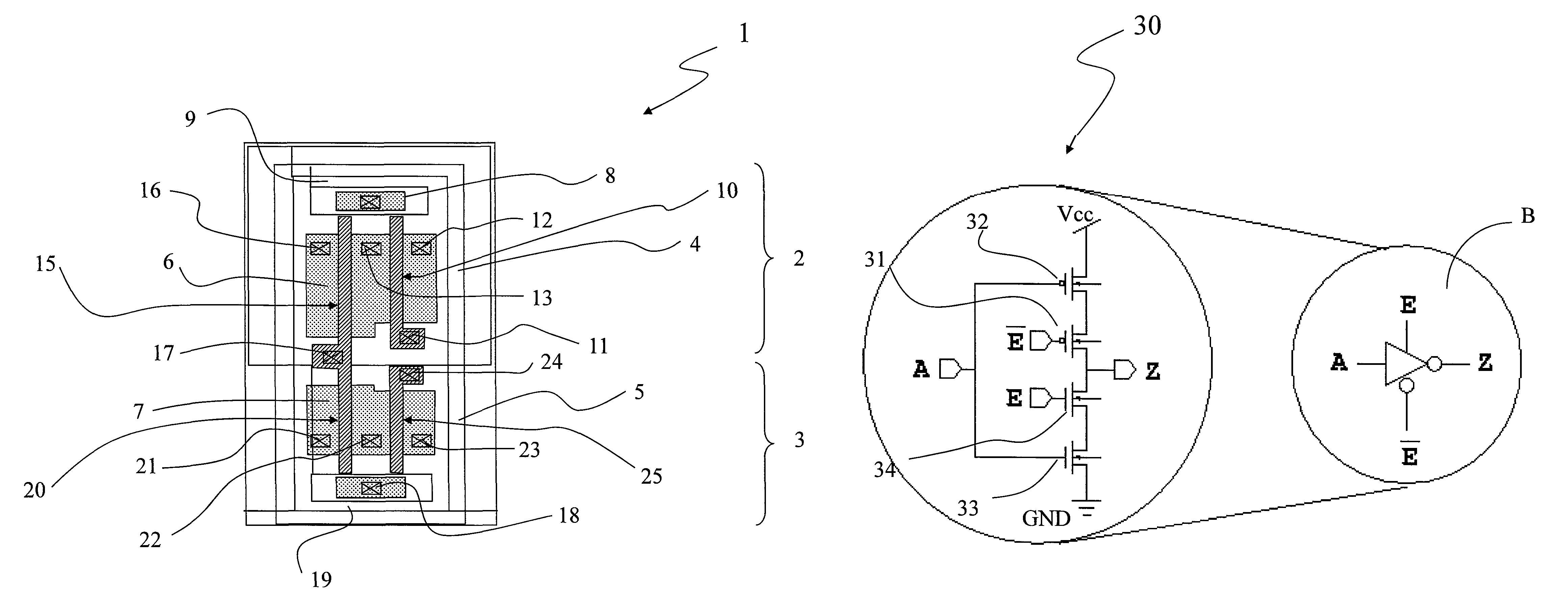
[0041]Furthermore, the complex functional logic cell can advantageously implement a multiplexer using three of the base cells.

Problems solved by technology

These demands have made Integrated Circuit (IC) scales and designs increasingly complex and time consuming.
In particular, physical layout takes up a major portion of the cycle of designing an Application Specific Integrated Circuit (ASIC).
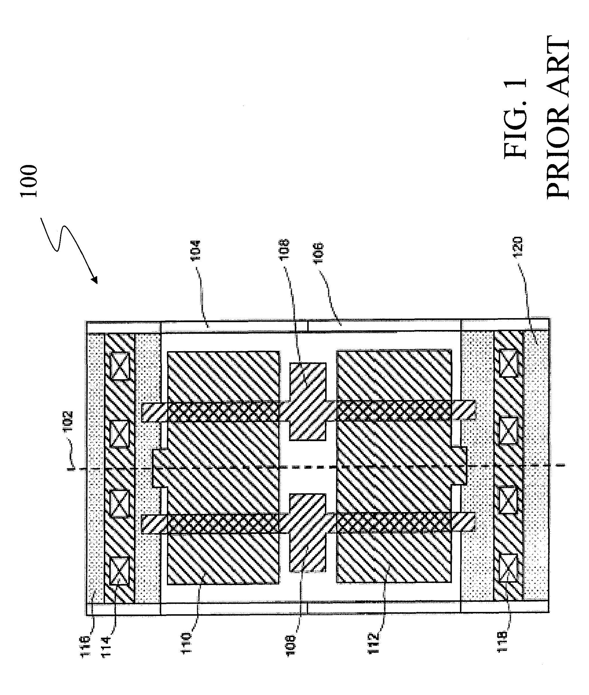
However, due to limitations inherent in the software environment, the place-and-route CAD tool requires that these extra logic cells be of the predefined types and numbers.
Such inflexibility may cause negative consequences.
For instance, in adding logic elements as required under an ECO, a logic cell of a certain type may not be available for implementing a desired function.
Moreover, it is a painful and time-consuming task to identify the extra logic cells and provide the proper wiring to properly connect the added cells.
Because of the increasing complexity of the IC design and modification, the turn-around time to incorporate the desired ECO changes is generally high.
The modification of metal contact layers is a drawback of this known solution because it does not sufficiently reduce the costs and the fabrication time of the products.
As a consequence, the construction of some complex cells, like three-state buffers, needs a very expensive implementation in terms of area occupation and an increase in the number of basic cells.
This area increase reduces the flexibility of the ECO implementation and the number of logic cells available, increasing the routing resources needed in the ECO implementation, this being a very critical problem for design development.
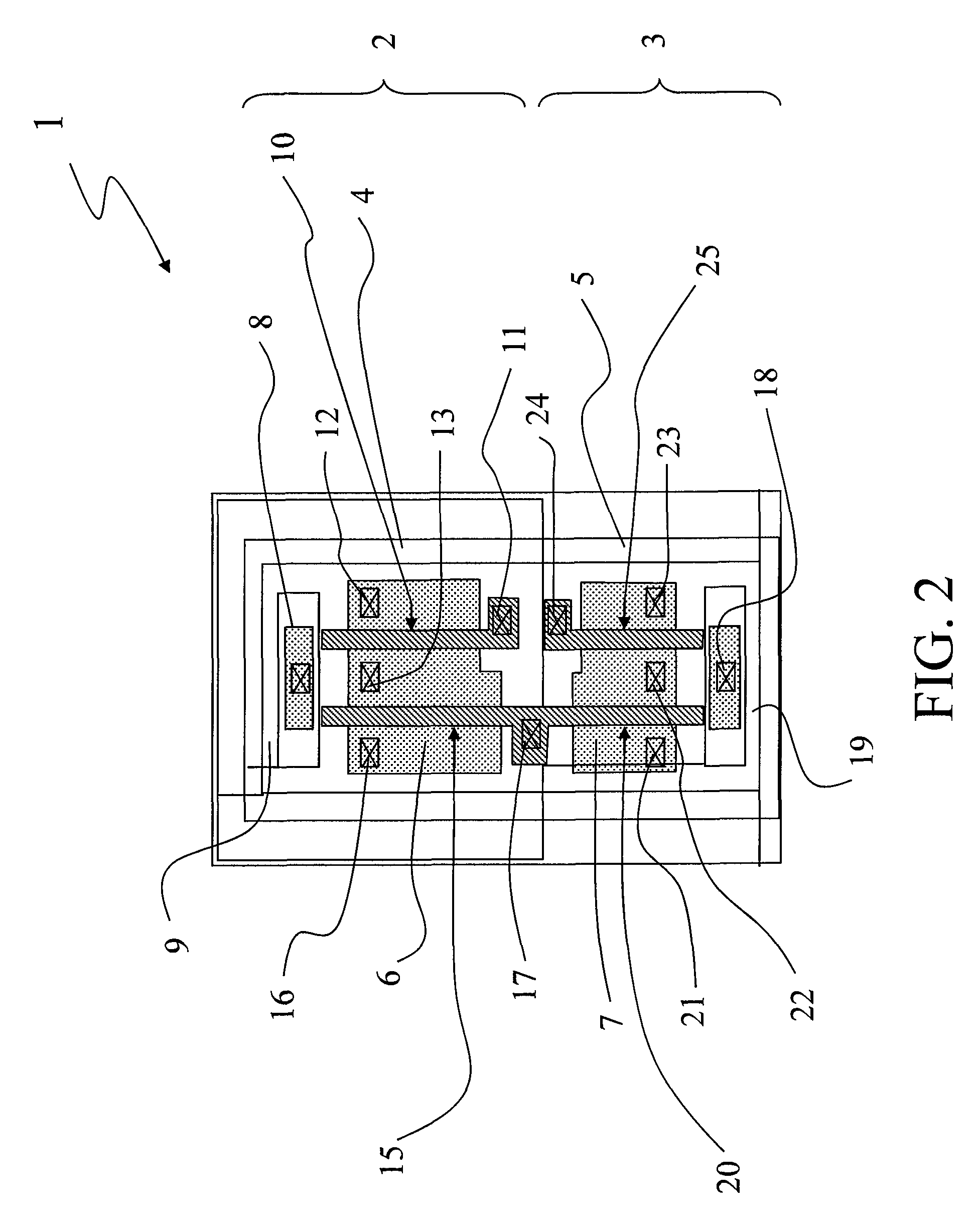
The technical problem of the present disclosure is to provide a base cell layout for an Engineering Change Order (ECO) implementation having structural and functional features that provide a reduction in design revision time and costs, overcoming the limitations and drawbacks of the known solutions.

Method used


Image

  • Base cell for engineering change order (ECO) implementation
  • Base cell for engineering change order (ECO) implementation
  • Base cell for engineering change order (ECO) implementation

Examples


Embodiment Construction

[0054]Referring specifically to FIG. 2, a top view of a layout of a base cell 1 for an Engineering Change Order (ECO) implementation according to the present disclosure is shown. It should be noted that the base cell 1 is asymmetrical because of the lack of a virtual center line, with respect to which all patterns of material layers are symmetrically mirrored. In particular, according to this embodiment, the base cell 1 includes four devices such as NMOS transistors and PMOS transistors. A P side 2 and an N side 3 are thus defined in the base cell 1.

[0055]In particular, an N-well 4 provides a substrate wherein two PMOS transistors are formed and a P-well 5 provides a substrate wherein two NMOS transistors are formed. A P+ region 6 and an N+ region 7 are implanted on the substrates provided respectively by the N-well 4 and the P-well 5. In particular, the P+ implant of the P+ region 6 forms the source and drain regions of the PMOS transistors, as well as the N+ implant of the N+ regi...


PUM


Abstract

A base cell for an Engineering Change Order (ECO) implementation having at least a first pair of CMOS transistors and a second pair of CMOS transistors, characterized in that said at least first pair of CMOS transistors have a common gate and said at least second pair of CMOS transistors have separate gates.

Description

BACKGROUND[0001]1. Technical Field[0002]The present disclosure relates to a base cell for an Engineering Change Order (ECO) implementation and, more particularly but non exclusively, relates to a mask programmable base cell for Engineering Change Order (ECO) post-silicon implementation, and the following description refers to this application field only to simplify the explanation.[0003]2. Description of the Related Art[0004]As it is well known, demands of consolidating functions and applications from printed circuit board to a single chip are growing stronger. These demands have made Integrated Circuit (IC) scales and designs increasingly complex and time consuming. For this reason, Computer-Aided Design (CAD) has become a necessary tool to speed up and improve the quality of IC design. In particular, physical layout takes up a major portion of the cycle of designing an Application Specific Integrated Circuit (ASIC).[0005]In creating a physical layout of an ASIC, a computer layout ...

Claims


Application Information

Patent Timeline
Patent Type & Authority Patents(United States)
IPC IPC(8): H01L25/00H03K19/00
CPCG06F17/5068H01L27/11807H01L27/0207G06F30/39
Inventor CICCARELLI, LUCACALI, LORENZOINNOCENTI, MASSIMILIANOMUCCI, CLAUDIONARDONE, VALENTINAPIZZOTTI, MATTEOROHILLA, PANKAJ
Owner STMICROELECTRONICS SRL
Learn More