Solid-state imaging apparatus
a technology of solid-state imaging and imaging apparatus, which is applied in the direction of solid-state devices, television systems, radioation controlled devices, etc., can solve problems such as degrading image quality
- Summary
- Abstract
- Description
- Claims
- Application Information
AI Technical Summary
Benefits of technology
Problems solved by technology
Method used
Image
Examples
first embodiment
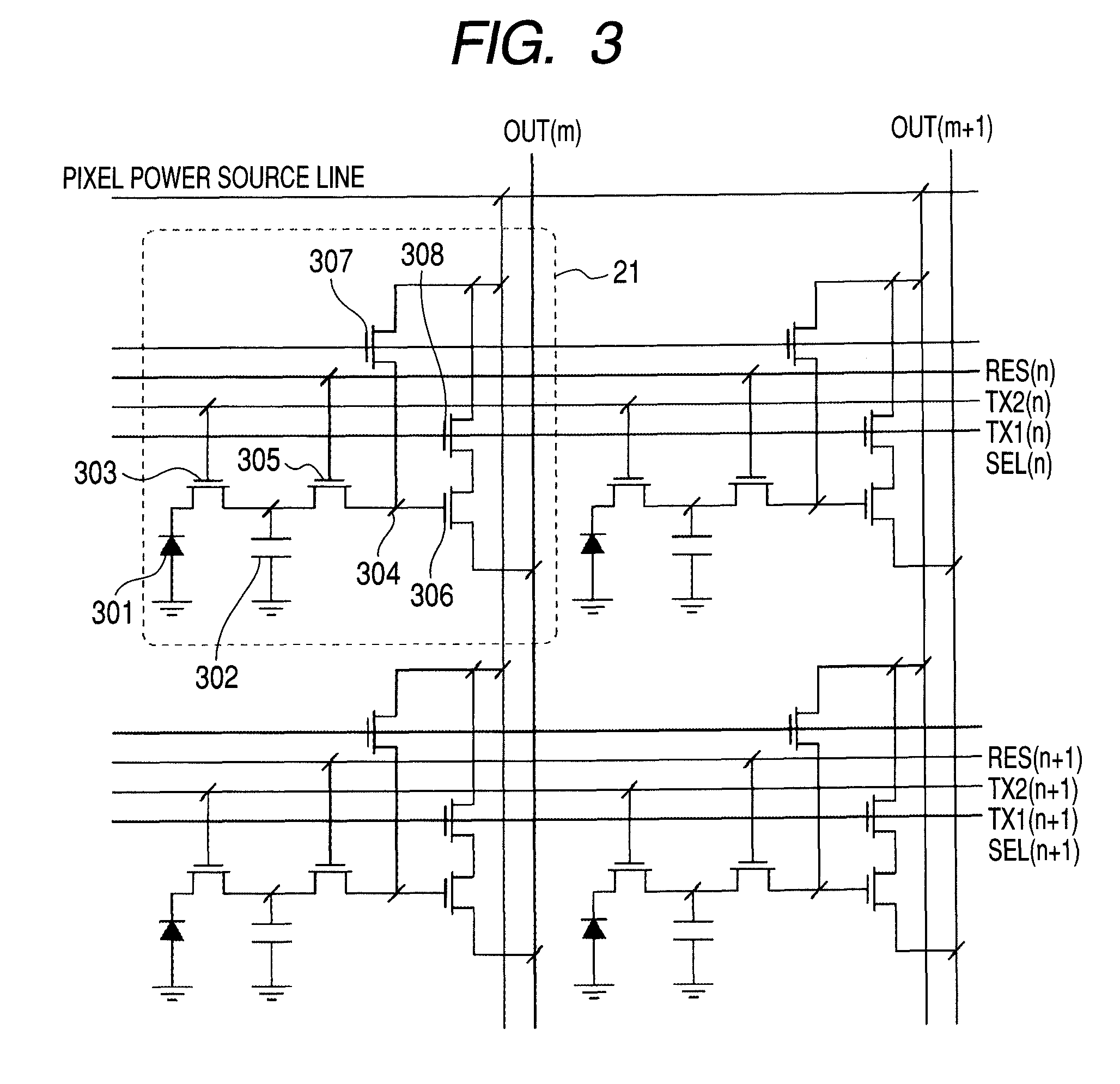
[0029]The first embodiment is described with reference to FIGS. 1 to 5.
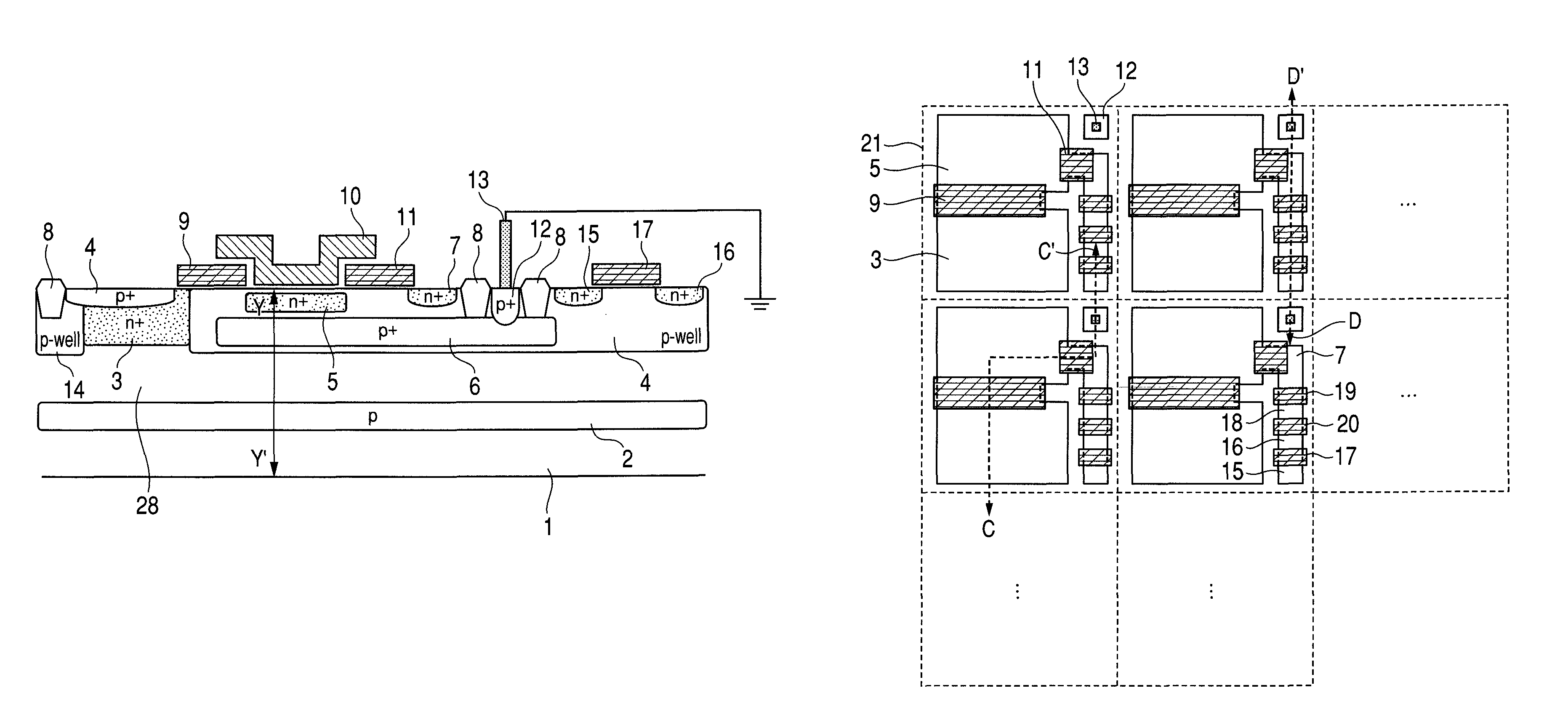
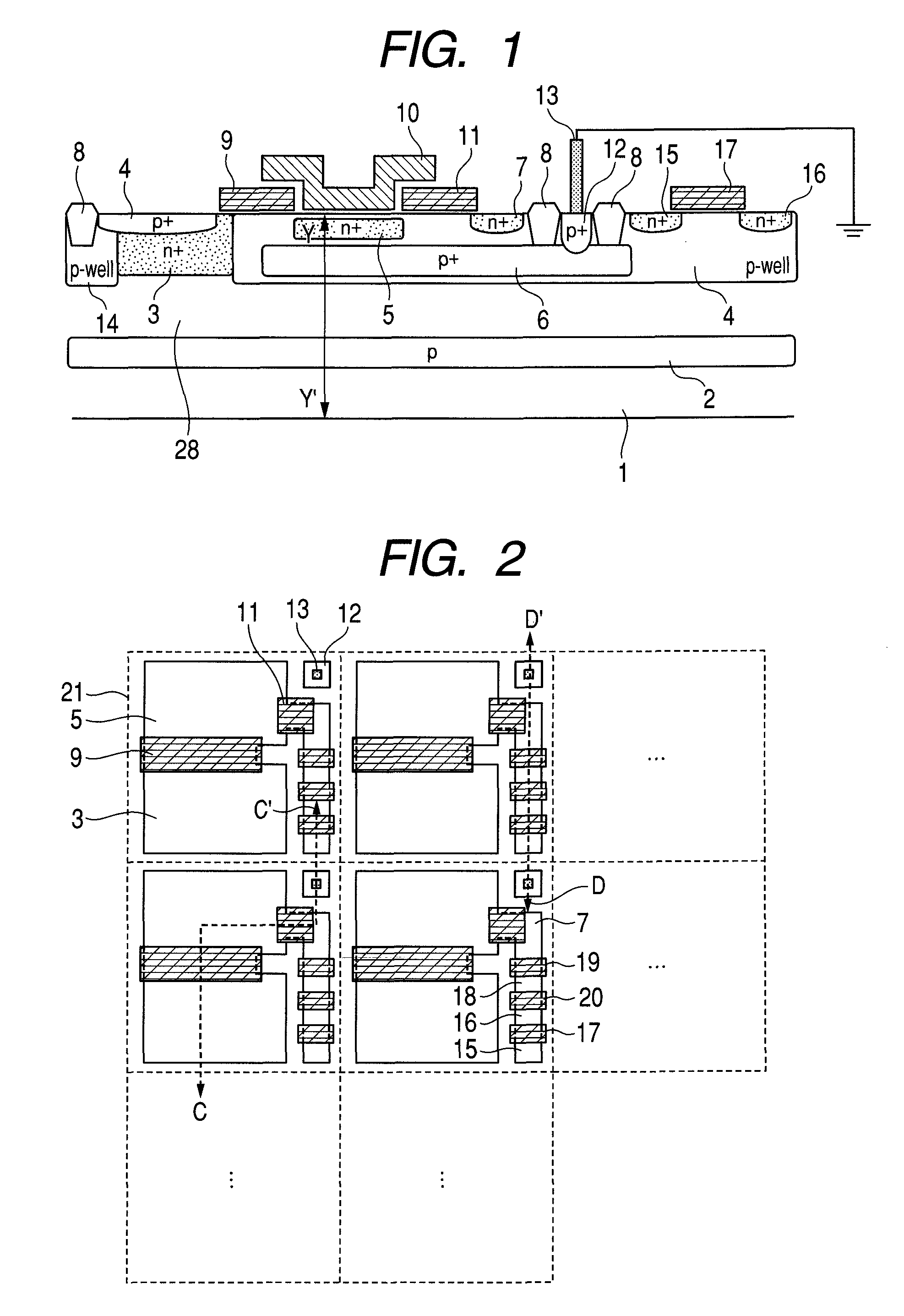
[0030]FIG. 1 is a schematic cross section of a solid-state imaging apparatus according to the present embodiment. The solid-state imaging apparatus includes an N-type semiconductor substrate 1 and a P-type semiconductor region (a fourth semiconductor region) 2 and the P-type semiconductor region 2 is called buried layer because it is buried deeply in a position below the surface of the substrate. The buried layer 2 extends between the semiconductor substrate 1 and an element arrangement surface region where a photoelectric conversion region and a carrier accumulation region are arranged and serves as a potential barrier against a signal carrier.
[0031]An N-type semiconductor region (a first semiconductor region) 3 and a P-type semiconductor region 4 form parts of the photoelectric conversion region respectively. The N-type semiconductor region 3 is a region (the same in polarity as the signal carrier) which is cap...
second embodiment
[0052]The second embodiment is described with reference to FIGS. 1, 2 and 6.
[0053]FIG. 6 is a cross section taken along with the line C-C′ of FIG. 2. The present embodiment is different from the first embodiment in that the potential barrier 6 is more extensive than the potential barrier 6 in the first embodiment, but the P well 14 is not arranged. Specifically, the potential barrier 6 is arranged under the FD region 7 and the source and the drain region 15 and 16 of the amplifying transistor. The potential barrier 6 may extend to under the source and the drain region of other MOS transistors. In such a configuration, if a potential on the source and the drain region of each MOS transistor varies during the operation of the VOFD function, a potential on the potential barrier 6 varies. However, the reference voltage is supplied to the potential barrier 6 through the P-type semiconductor region 12 to allow variation in potential to be reduced.
[0054]As is the case with the first embodi...
third embodiment
[0056]The third embodiment is described with reference to FIGS. 1, 2 and 7.
[0057]FIG. 7 is a cross section taken along with the line C-C′ of FIG. 2. The present embodiment is different from the first and the second embodiment in that a P-type semiconductor region 22 is further arranged under the P-type semiconductor region 6. FIG. 7 makes a description with reference to an example of configuration of the first embodiment. The P-type semiconductor region 22 is lower in impurity concentration than the potential barrier 6. A potential on the buried layer 2 is fixed at the outer periphery outside the pixel region.
[0058]In a case where the N-type semiconductor region 28 is arranged between the buried layer 2 and the potential barrier 6 like FIG. 1 to operate the VOFD, variation in potential on the buried layer 2 is prevented from being transferred to the potential barrier 6 due to capacitive coupling between the buried layer 2 and the potential barrier 6.
[0059]If any variation in potenti...
PUM
 Abstract
Description
Claims
Application Information
 - R&D
- Intellectual Property
- Life Sciences
- Materials
- Tech Scout
- Unparalleled Data Quality
- Higher Quality Content
- 60% Fewer Hallucinations
Browse by: Latest US Patents, China's latest patents, Technical Efficacy Thesaurus, Application Domain, Technology Topic, Popular Technical Reports.
© 2025 PatSnap. All rights reserved.Legal|Privacy policy|Modern Slavery Act Transparency Statement|Sitemap|About US| Contact US: help@patsnap.com


