
Integrated thin-film solar cells and method of manufacturing thereof and processing method of transparent electrode for integrated thin-film solar cells and structure thereof, and transparent substrate having processed transparent electrode

a technology of integrated thin-film solar cells and manufacturing methods, applied in the manufacture of final products, other domestic articles, optical articles, etc., can solve the problems the efficiency of converting energy is reduced, and the process cannot help but act as a factor of increasing the cost of solar cells, so as to reduce manufacturing costs, maximize the effective area of solar cells, and improve the performance of solar cells

Inactive Publication Date: 2011-04-19
KOREA ADVANCED INST OF SCI & TECH
View PDF36 Cites 16 Cited by
  • Summary
  • Abstract
  • Description
  • Claims
  • Application Information

AI Technical Summary

Benefits of technology

[0054]As described above, according to the present invention, a (insulating) gap between unit cells of the integrated thin film solar cells can be reduced by several tens of times or more as compared to existing laser patterning and chemical vaporization machining methods. Thus, the effective area of the solar cells can be maximized, and accordingly the performance of the module of the solar cells can be improved.
[0055]Furthermore, no precise position control apparatus is required because self-aligning is possible, and no expensive equipment such as a laser, precision position control system and the like is required as etching is performed by using a printing method at the time of processing a transparent electrode, thus reducing manufacturing costs. Further, since every process after the formation of the transparent electrode is carried out in vacuum, it is possible to prevent the performance of the solar cell module from degrading by an exposure to the atmosphere.

Problems solved by technology

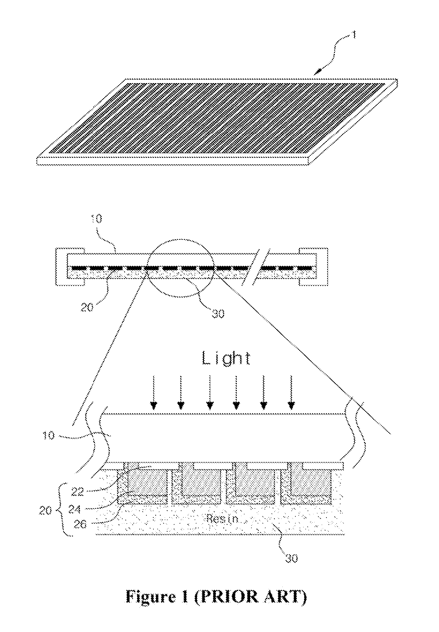
However, with a rapid increase of the demand for bulk silicon solar cells in recent years, there is a tendency that the costs are increasing due to the shortage of materials.
But, as the area of the thin film solar cells are larger, the efficiency of the converting energy is reduced because of the resistance of the transparent electrode.
However, there are other problems in the structure and manufacturing process of intergrated thin film solar cells.
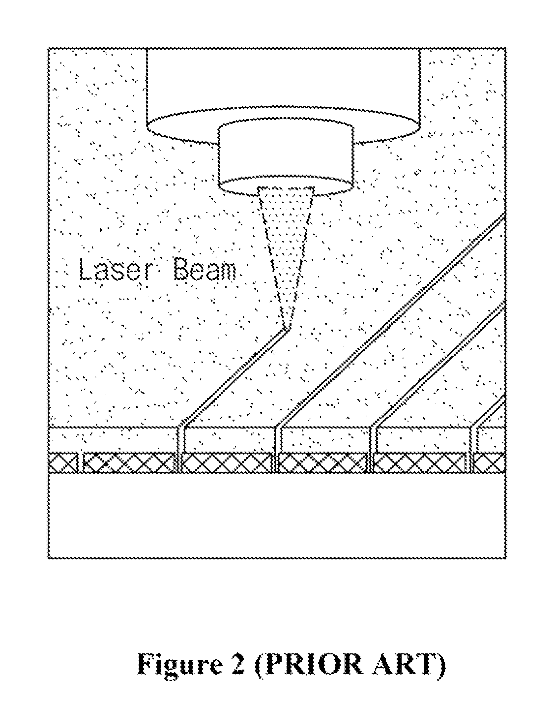
Problems of such laser patterning method are to be noted.
As a result, such a process cannot help but act as a factor of increasing the cost of the solar cells.
Further, since the substrate is exposed to the air for etching the solar cell layer 24, there may happen to a problem that the characteristics of the solar cell module are degraded due to adhesion of moisture and contaminants.
Such a process also may cause the aforementioned problems in process discontinuity and contamination.
Thus the effective area loss of the solar cells is increased.
Moreover, the laser equipment for patterning is expensive, and a precision position control system is required for patterning at a precise position.
Due to this, the manufacturing cost increases.
This emerges as a very difficult problem when it is intended to manufacture integrated solar cells using a large area substrate.
Further, the gap that can be etched is about 200 μm to the smallest, which is greater than a (insulating) gap formed by the laser patterning method, and thus the loss of the effective area of the solar cells is increased.
However, the existing mechanical scribing method is also limited to use with a solar cell (semiconductor) layer.
Thus, there is a problem that laser patterning equipment and a precision position control apparatus or the like for precise position control are required so as to etch molybdenum (Mo) used as a back electrode and zinc oxide (ZnO) used as a front electrode.

Method used


Image

  • Integrated thin-film solar cells and method of manufacturing thereof and processing method of transparent electrode for integrated thin-film solar cells and structure thereof, and transparent substrate having processed transparent electrode
  • Integrated thin-film solar cells and method of manufacturing thereof and processing method of transparent electrode for integrated thin-film solar cells and structure thereof, and transparent substrate having processed transparent electrode
  • Integrated thin-film solar cells and method of manufacturing thereof and processing method of transparent electrode for integrated thin-film solar cells and structure thereof, and transparent substrate having processed transparent electrode

Examples


Embodiment Construction

[0072]FIG. 3 is a cross sectional view illustrating a structure of integrated thin film solar cells according to the present invention. As illustrated therein, the integrated thin film solar cells according to the present invention is constructed of a structure in which a transparent electrode 2 having a sloped section over a predetermined substrate 1, a solar cell (semiconductor) layer 3, a first back electrode 4 and a second back electrode 5 are sequentially stacked.

[0073]That is, the transparent electrode 2 is formed with a (insulating) gap, being patterned such that left and right adjacent transparent electrodes 2 can be insulated from each other, the solar cell (semiconductor) layer 3 and the first back electrode 4 are deposited over the patterned transparent electrode 2, the second back electrode 5 positioned over the first back electrode 4 is contacted with the adjacent transparent electrode at one side, thus electrically connecting unit devices in series.

[0074]A patterned si...


PUM


Abstract

The present invention relates to integrated thin film solar cells, and more particularly, to integrated thin film solar cells, which minimize the loss of integrated solar cells caused at the time of a manufacturing process and become available at a low cost process, and a method of manufacturing thereof, a processing method of a transparent electrode for integrated thin film solar cells, which widens an effective area and reduces manufacturing costs by minimizing a (insulating) gap between unit cells of the integrated thin film solar cells, and a structure thereof, and a transparent substrate having the transparent electrode. The method of manufacturing integrated thin film solar cells, comprising the steps of: (a) forming a transparent electrode pattern separately over a transparent substrate; (b) forming a solar cell (semiconductor) layer over the substrate of the step (a); (c) forming a first back electrode by obliquely depositing a conductive material over the solar cell (semiconductor) layer; (d) etching the solar cell (semiconductor) layer by using the first back electrode as a mask; and (e) forming a second back electrode so that the transparent electrode and the first back electrode are electrically connected by obliquely depositing a metal over the substrate of the step (d).

Description

TECHNICAL FIELD[0001]The present invention relates to integrated thin film solar cells, and more particularly, to integrated thin film solar cells, which minimize the loss of the area of the integrated solar cells caused at the time of a manufacturing process and become available at a low cost process, and a method of manufacturing thereof, to a processing method of a transparent electrode for integrated thin film solar cells having a plurality of unit cells insulated at regular gaps and made into a module by electrically serial connection, which minimize a (insulating) gap between the unit cells, and a structure thereof, and a transparent substrate having the transparent electrode.BACKGROUND ART[0002]Solar cells are semiconductor devices that convert the energy of sunlight directly into electricity. They can be roughly divided into silicon-based solar cells, compound-based solar cells and organic-based solar cells based on the material to be used.[0003]Silicon solar cells are subdi...

Claims


Application Information

Patent Timeline
Patent Type & Authority Patents(United States)
IPC IPC(8): H01L31/04H01L31/18
CPCH01L31/022466H01L31/1804H01L31/046H01L31/1884Y02E10/547H01L31/0463Y02P70/50
Inventor LIM, KOENG SUKWON, SEONG WONKWAK, JEONG HWANPARK, SANG ILYOON, JUN-BOMOON, GUN-WOO
Owner KOREA ADVANCED INST OF SCI & TECH
Learn More