Probe apparatus with mechanism for achieving a predetermined contact load
a technology of contact load and probe apparatus, which is applied in the direction of measurement device, semiconductor/solid-state device testing/measurement, instruments, etc., can solve the problems of deteriorating the reliability of test, and not being able to cope with deformation of interface parts including the probe card and the head-plate during test, and achieves high-reliability test
- Summary
- Abstract
- Description
- Claims
- Application Information
AI Technical Summary
Benefits of technology
Problems solved by technology
Method used
Image
Examples
first embodiment
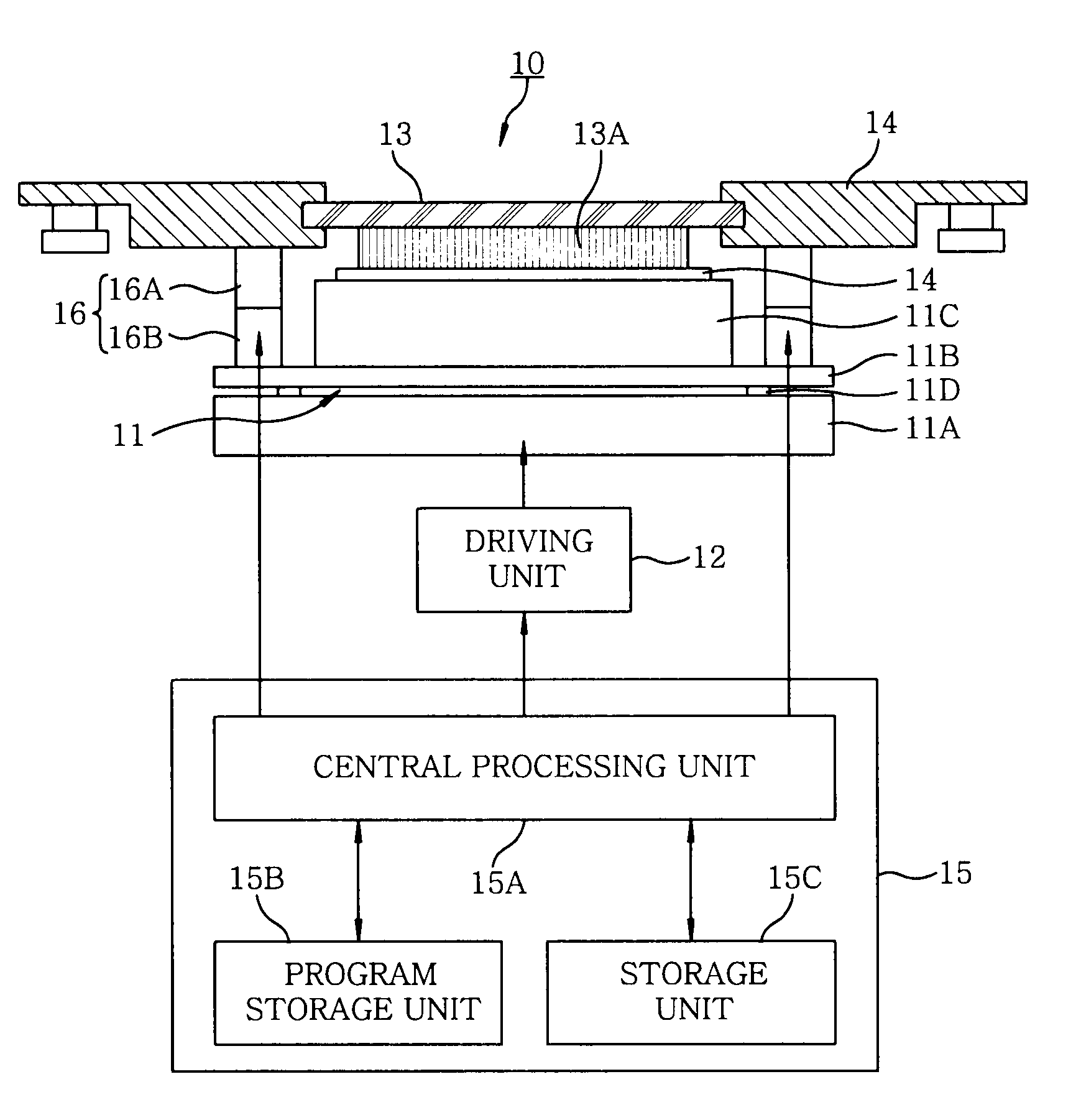
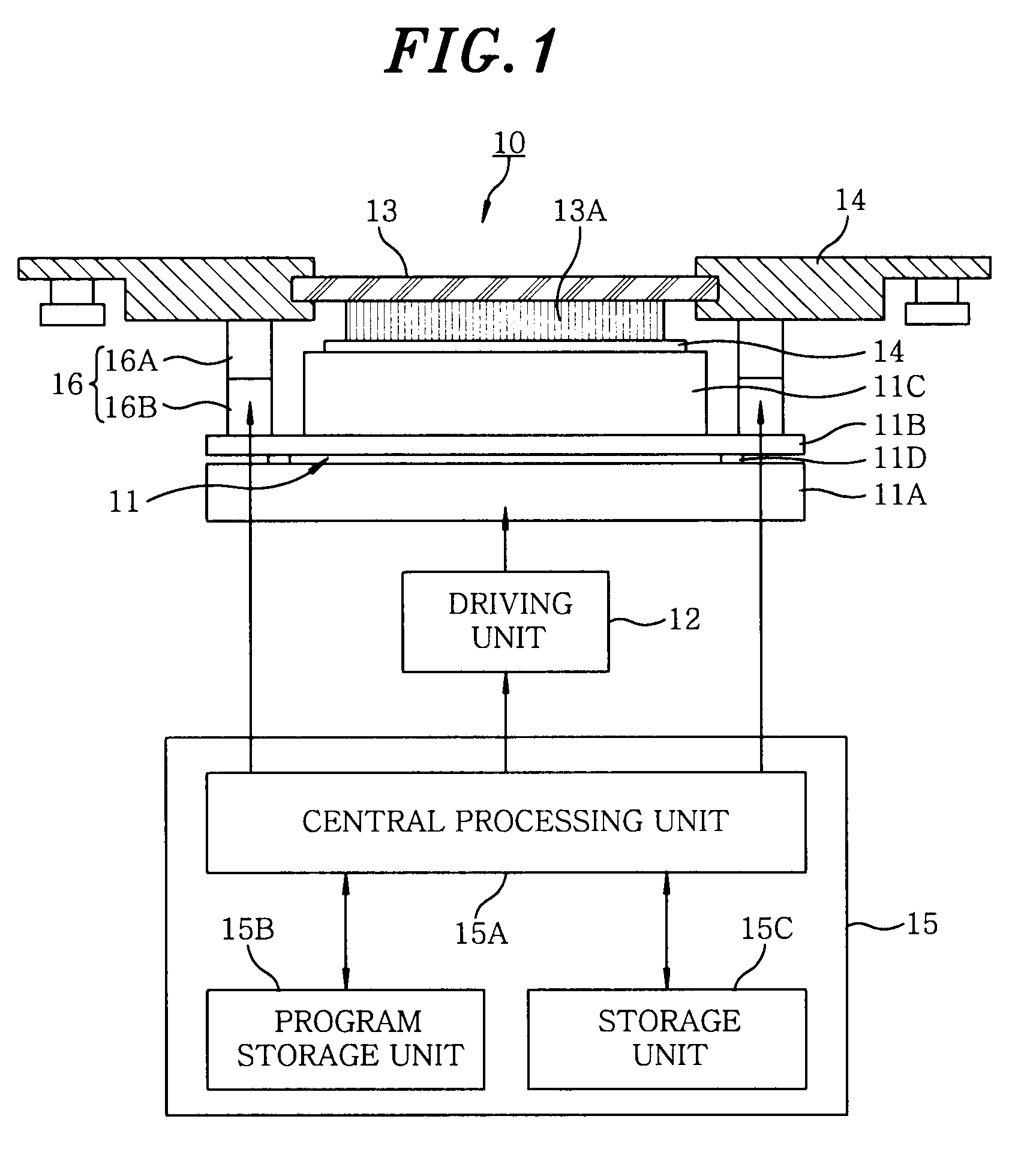
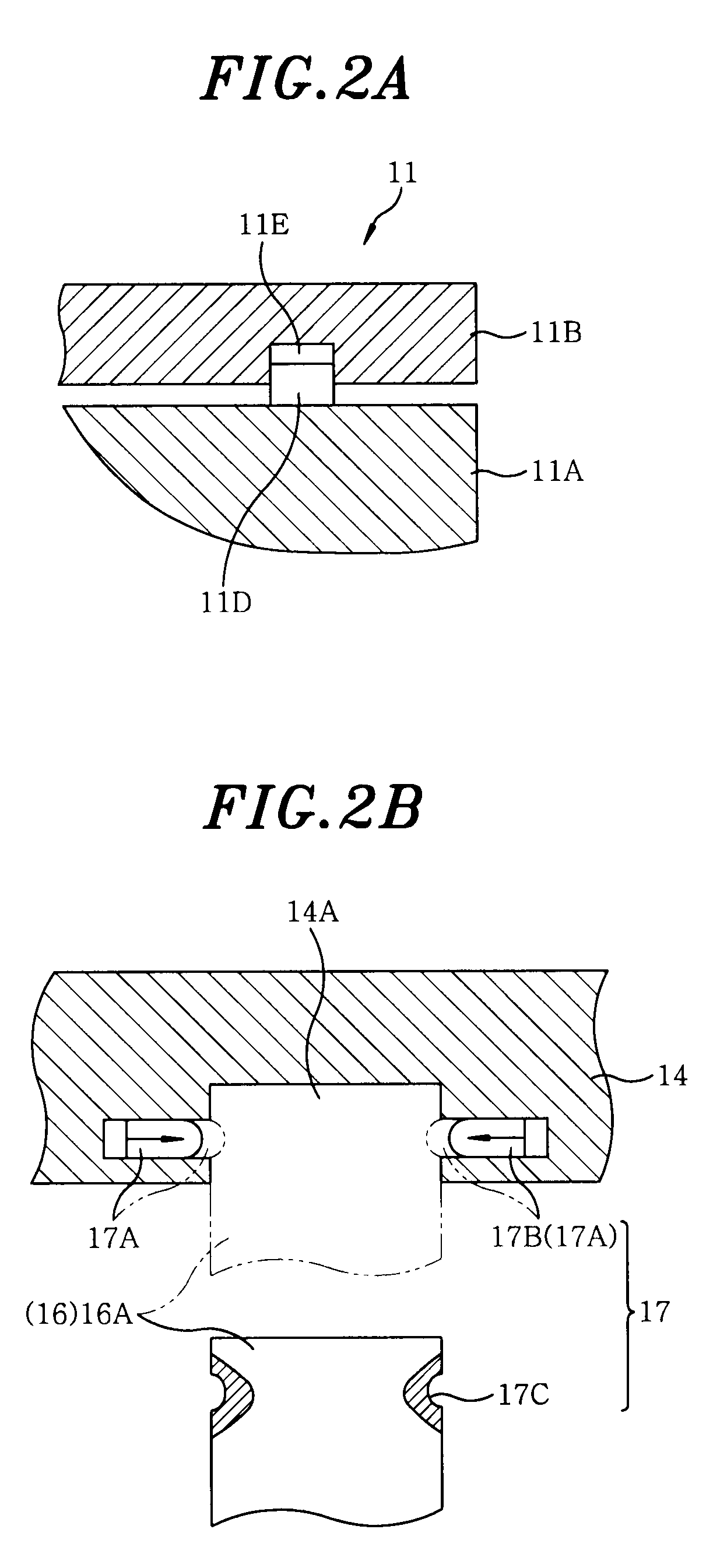
[0024]First, a probe apparatus 10 in accordance with the first embodiment will be described with reference to FIG. 1. The probe apparatus 10 of the first embodiment, for example, as shown in FIG. 1, includes: a mounting table 11 on which an object to be tested (for example, a semiconductor wafer W) is mounted, the mounting table 11 being movable in directions of X, Y, Z and ⊖; a drive mechanism 12 to move the mounting table 11 in directions of X, Y, Z and ⊖; a probe card 13 arranged above the mounting table 11 and having a plurality of probes 13A to come into contact with a plurality of electrode pads of the semiconductor wafer W; a supporting member (for example, a head-plate) 14 to horizontally support the probe card 13; and a control unit 15 to control various components including the mounting table 11. In this probe apparatus, under the control of the control unit 15, the mounting table 11 is overdriven by a predetermined distance to allow the electrode pads of the semiconductor...
second embodiment
[0041]A probe apparatus 10A in accordance with the second embodiment, for example, as shown in FIGS. 5A to 5C, is approximately identical to that of the first embodiment except for the mounting table 11. Accordingly, in the following description, the constituent elements of the second embodiment that are equal to or corresponding to those of the first embodiment are respectively designated by the same reference numerals, and they are described based on the configuration of the second embodiment. FIGS. 5A to 5C correspond to FIGS. 3A to 3C, respectively.
[0042]More specifically, as shown in FIGS. 5A to 5C, the mounting table 11 of the second embodiment has an integral configuration and is movable in directions of X, Y, Z and ⊖ by the drive mechanism. The mount 11C on which the semiconductor wafer W is mounted is provided at an upper surface of the mounting table 11, and the cylinder mechanisms 16 are provided at radially outer positions, i.e., on an outer peripheral region of the uppe...
PUM
 Abstract
Description
Claims
Application Information
 - R&D
- Intellectual Property
- Life Sciences
- Materials
- Tech Scout
- Unparalleled Data Quality
- Higher Quality Content
- 60% Fewer Hallucinations
Browse by: Latest US Patents, China's latest patents, Technical Efficacy Thesaurus, Application Domain, Technology Topic, Popular Technical Reports.
© 2025 PatSnap. All rights reserved.Legal|Privacy policy|Modern Slavery Act Transparency Statement|Sitemap|About US| Contact US: help@patsnap.com


