
Carrier phase and symbol timing recovery circuit for an ATSC receiver and method of recovering a carrier phase and a symbol timing in received digital signal data

a carrier phase and symbol timing technology, applied in the direction of digital transmission, television signal transmission by single/parallax channel, synchronisation signal speed/phase control, etc., can solve the problem of not being able to design a symbol phase recovery circuit completely, and it is difficult for conventional recovery circuits to completely separate the carrier phase recovery process

Active Publication Date: 2010-09-21
SAMSUNG ELECTRONICS CO LTD
View PDF10 Cites 5 Cited by
  • Summary
  • Abstract
  • Description
  • Claims
  • Application Information

AI Technical Summary

Benefits of technology

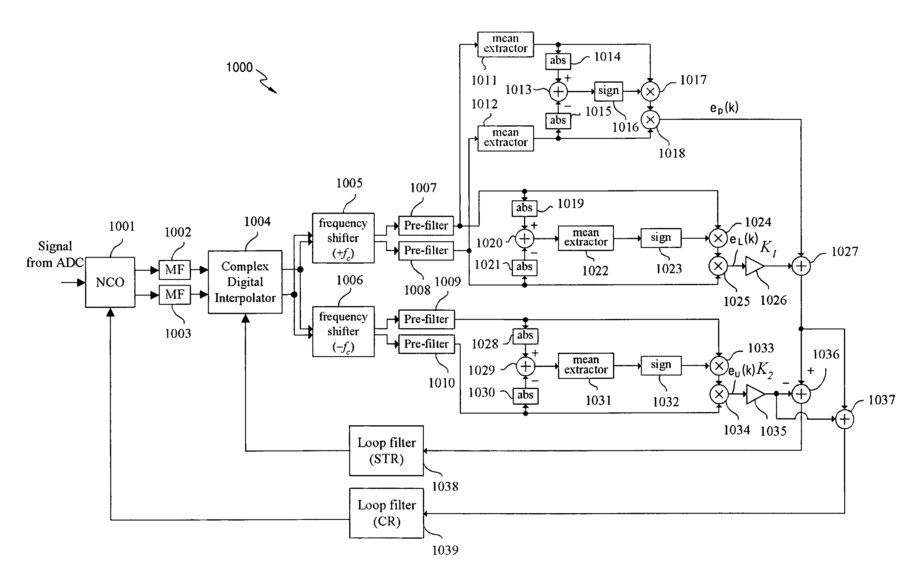
The present invention provides a circuit and method for simultaneously recovering a carrier phase and a symbol timing in received digital signal data. The circuit includes an error detector and addition / subtraction units to determine carrier phase and symbol timing offsets based on detected phase errors. The desired sampling time instant and carrier phase offset can be detected at a point where the carrier phase and symbol timing offset values are each zero. The technical effect of the invention is to improve the accuracy and reliability of carrier phase and symbol timing recovery in received digital signal data.

Problems solved by technology

Therefore, it may be substantially difficult to design a phase recovery circuit which does not depend on a symbol timing offset.
Similarly, it is not possible to design a symbol timing recovery circuit completely independent of a phase offset.
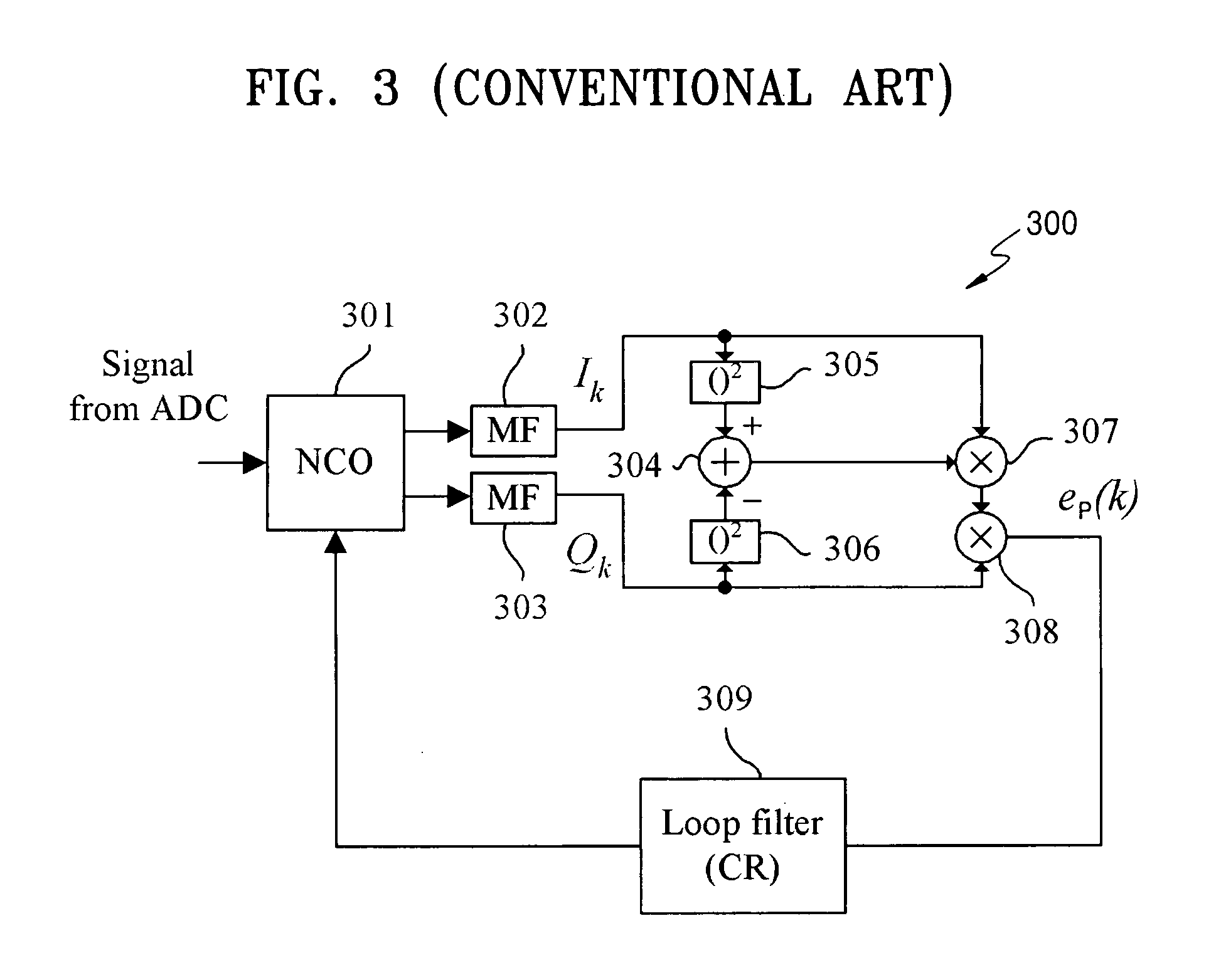
However, it is difficult for conventional recovery circuits to completely separate the carrier phase recovery process from the symbol timing recovery process.

Method used


Image

  • Carrier phase and symbol timing recovery circuit for an ATSC receiver and method of recovering a carrier phase and a symbol timing in received digital signal data
  • Carrier phase and symbol timing recovery circuit for an ATSC receiver and method of recovering a carrier phase and a symbol timing in received digital signal data
  • Carrier phase and symbol timing recovery circuit for an ATSC receiver and method of recovering a carrier phase and a symbol timing in received digital signal data

Examples


Embodiment Construction

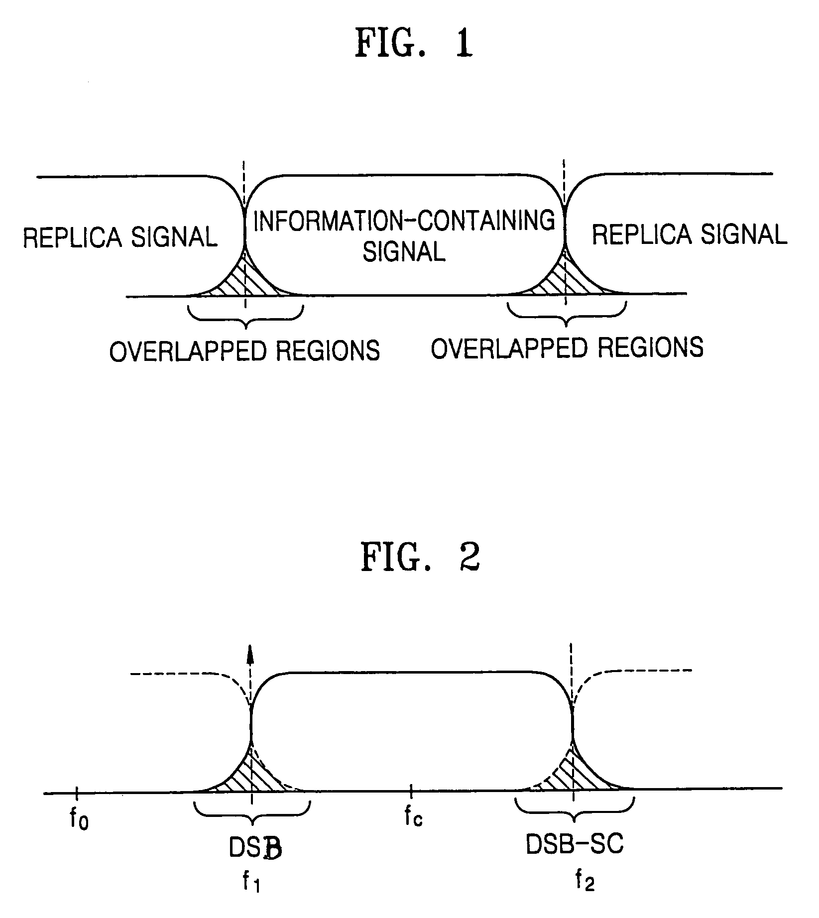
[0028]As will be described in more detail below, example embodiments of the present invention may provide a carrier phase and symbol timing recovery circuit for an ATSC receiver, and method for recovering a carrier phase and a symbol timing in received digital signal data. The example circuits and method may be capable of performing a carrier phase and symbol timing recovery process jointly (i.e., simultaneously) without having to avoid correlation between carrier phase and symbol timing recovery circuits. The example circuits and methodology may use all the redundancy information existing in an ATSC signal for both carrier phase and symbol timing synchronizations, so as to simultaneously perform carrier phase and symbol timing recovery processes in the ATSC receiver. The redundancy information may exist in a pilot signal, an upper overlapped region and a lower overlapped region.

[0029]The pilot signal may be embodied as a high-power impulse signal added to each data symbol in order ...


PUM


Abstract

A carrier phase and symbol timing recovery circuit and method may be used for robust synchronization in a broadcasting ATSC receiving system. Carrier phase and symbol timing offsets may be simultaneously adjusted by using redundancy information contained in an ATSC signal spectrum. A desired sampling time instant and carrier phase offset for synchronization may be simultaneously obtained due to correlation between carrier phase and symbol timing detectors.

Description

PRIORITY STATEMENT[0001]This application claims the priority of Korean Patent Application No. 10-2004-0079958, filed on Oct. 7, 2004, in the Korean Intellectual Property Office, the disclosure of which is incorporated herein in its entirety by reference.BACKGROUND OF THE INVENTION[0002]1. Field of the Invention[0003]The present invention is generally related to a carrier phase and symbol timing recovery circuit used for a High Definition Television (HDTV) receiver operating in accordance with a standard of the Advanced Television System Committee (ATSC), and to a method of recovering a carrier phase and a symbol timing in received digital signal data.[0004]2. Description of the Related Art[0005]ATSC receiving systems may be designed to operate even in severe multi-path environments, such as cities for example. In multi-path environments, substantially strong ghost signals may occur due to reflection of electromagnetic waves from buildings, etc. Therefore, in order to operate stably ...

Claims


Application Information

Patent Timeline
Patent Type & Authority Patents(United States)
IPC IPC(8): H04L27/00H03D3/18
CPCH04L7/0029H04L7/027H04L27/066H04L7/06H04L2027/0028H04L2027/0055H04L2027/0067H04L2027/0087H04N7/015H04L7/0278H04N7/12
Inventor ZHIDKOV, SERGEYKIM, MIN-HO
Owner SAMSUNG ELECTRONICS CO LTD
Learn More