Liquid crystal display and a defect correcting method for the same
a liquid crystal display and defect correction technology, applied in static indicating devices, instruments, non-linear optics, etc., can solve problems such as defective pixels and unintentional pixels, and achieve the effects of improving production efficiency, improving display quality, and reducing the number of defects
- Summary
- Abstract
- Description
- Claims
- Application Information
AI Technical Summary
Benefits of technology
Problems solved by technology
Method used
Image


Examples
first preferred embodiment
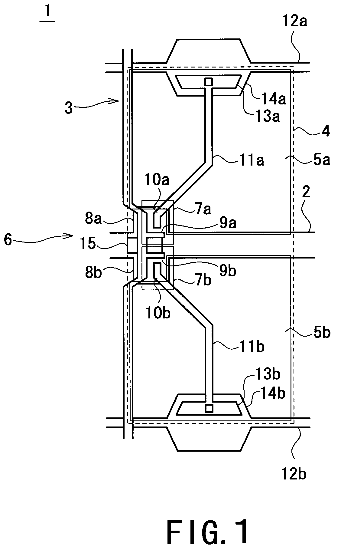
[0043]FIG. 1 is a schematic diagram showing a pixel electrode formed on an active matrix array substrate provided in a liquid crystal display according to a first preferred embodiment of the present invention.
[0044]On a transparent substrate (unillustrated) constituting the active matrix array substrate 1, a plurality of gate lines 2 extending in a row direction are formed, and a plurality of source lines 3 extending in a column direction are formed while intersecting at right angles with the gate lines 2 via an insulating layer (unillustrated). Incidentally, the gate line 2 shown in FIG. 1 is the nth one, and the source line 3 shown in FIG. 1 is the mth one. In addition, the gate line 2 is a lower-layer side line, and the source line 3 is an upper-layer side line.
[0045]A pixel electrode 4 is split into two sub-pixel electrodes 5a and 5b interposing the gate line 2 therebetween. In the vicinity of an intersection portion 6 of the gate line 2 and the source line 3, separate thin film...
second preferred embodiment
[0062]FIG. 9 is a schematic view showing a pixel electrode formed on an active matrix array substrate provided in a liquid crystal display according to a second preferred embodiment of the present invention.
[0063]The structure of the active matrix array substrate 30 provided in the liquid crystal display according to the second preferred embodiment is basically the same as the structure of the active matrix array substrate 1 provided in the liquid crystal display according to the first preferred embodiment except for the source line 3. Therefore, differences from the liquid crystal display and the defect correcting method for the same according to the first preferred embodiment will be mainly described hereinafter.
[0064]As shown in FIG. 9, in the active matrix array substrate 30 provided in the liquid crystal display according to the second preferred embodiment, an additional source line 32 is further included while being partially connected to the source line 3 via connecting porti...
third preferred embodiment
[0072]FIG. 11 is a schematic diagram showing a pixel electrode formed on an active matrix array substrate provided in a liquid crystal display according to the third preferred embodiment.
[0073]The structure of the active matrix array substrate 40 provided in the liquid crystal display according to the third preferred embodiment is also basically the same as the structure of the active matrix array substrate 1 provided in the liquid crystal display according to the first preferred embodiment except for the source line 3. Therefore, differences from the liquid crystal display and the defect correcting method for the same according to the first preferred embodiment will be mainly described hereinafter.
[0074]As shown in FIG. 11, in the active matrix array substrate 40 provided in the liquid crystal display according to the third preferred embodiment, a bypass line 41 is included in the vicinity of the opening portion 15 of the source line 3. In this preferred embodiment, an example of t...
PUM
| Property | Measurement | Unit |
|---|---|---|
| transparent | aaaaa | aaaaa |
| defect | aaaaa | aaaaa |
| size | aaaaa | aaaaa |
Abstract
Description
Claims
Application Information
 - R&D
- Intellectual Property
- Life Sciences
- Materials
- Tech Scout
- Unparalleled Data Quality
- Higher Quality Content
- 60% Fewer Hallucinations
Browse by: Latest US Patents, China's latest patents, Technical Efficacy Thesaurus, Application Domain, Technology Topic, Popular Technical Reports.
© 2025 PatSnap. All rights reserved.Legal|Privacy policy|Modern Slavery Act Transparency Statement|Sitemap|About US| Contact US: help@patsnap.com