Acceleration sensor device having piezo-resistors measuring acceleration
a sensor device and acceleration technology, applied in measurement devices, speed/acceleration/shock measurement, instruments, etc., can solve the problems of large offset voltage and flexible arms to be broken, and achieve the effect of reducing offset voltage, reducing damping period of oscillation, and facilitating transmission
- Summary
- Abstract
- Description
- Claims
- Application Information
AI Technical Summary
Benefits of technology
Problems solved by technology
Method used
Image
Examples
example 1
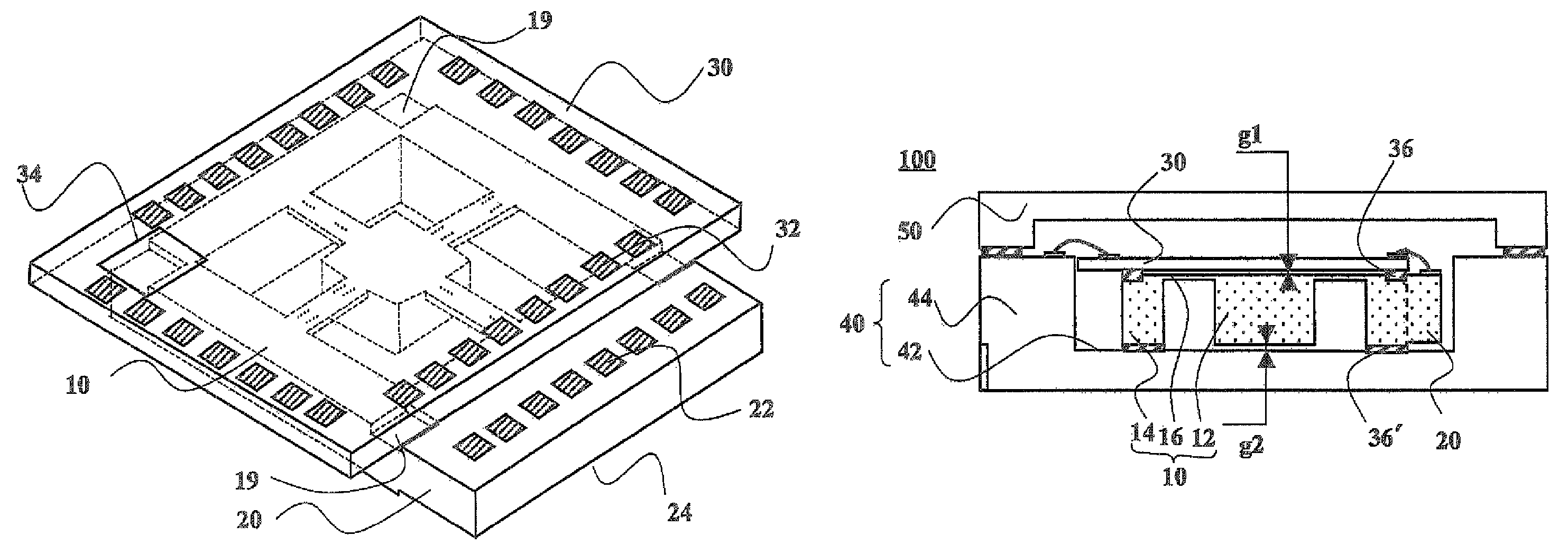
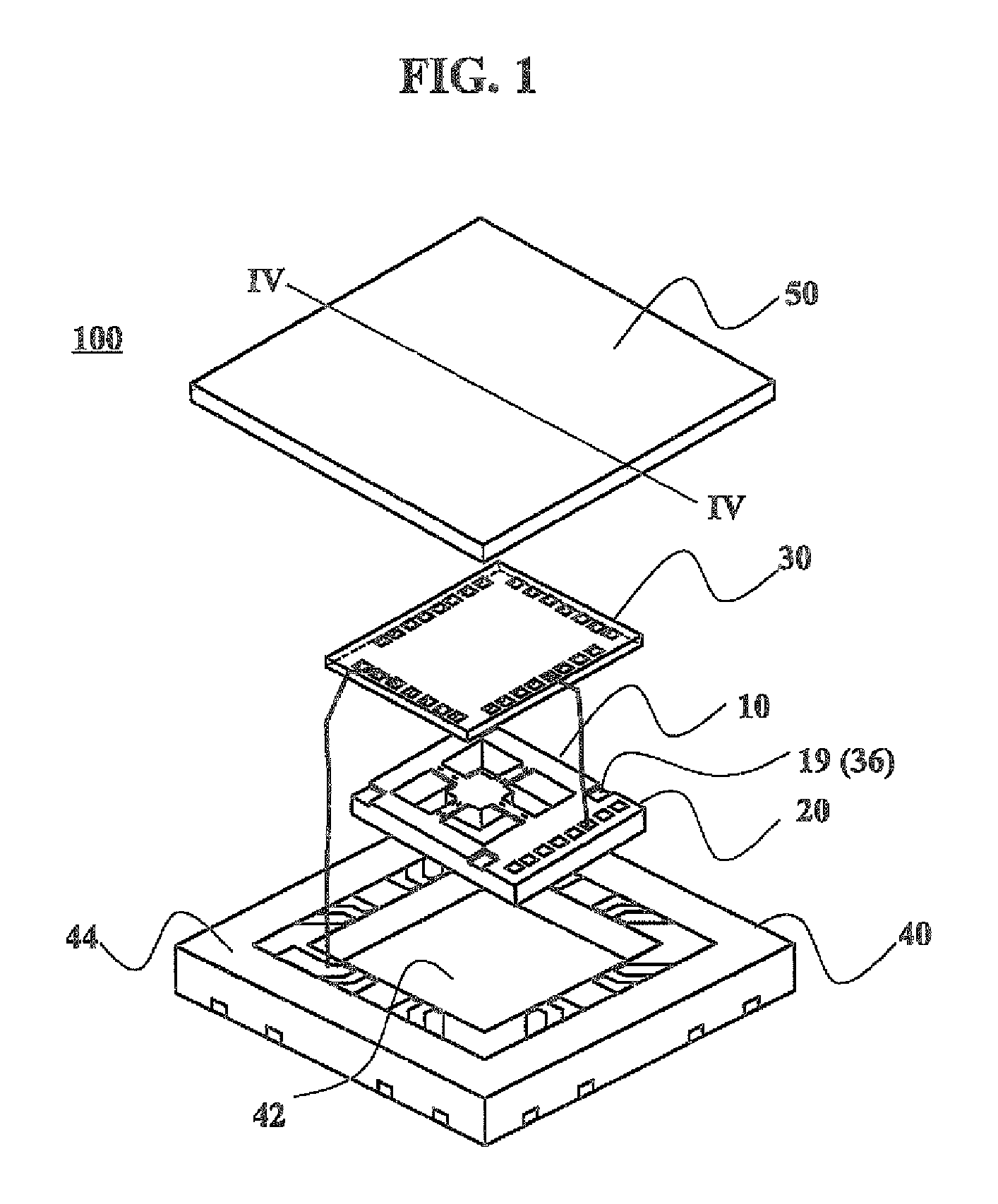
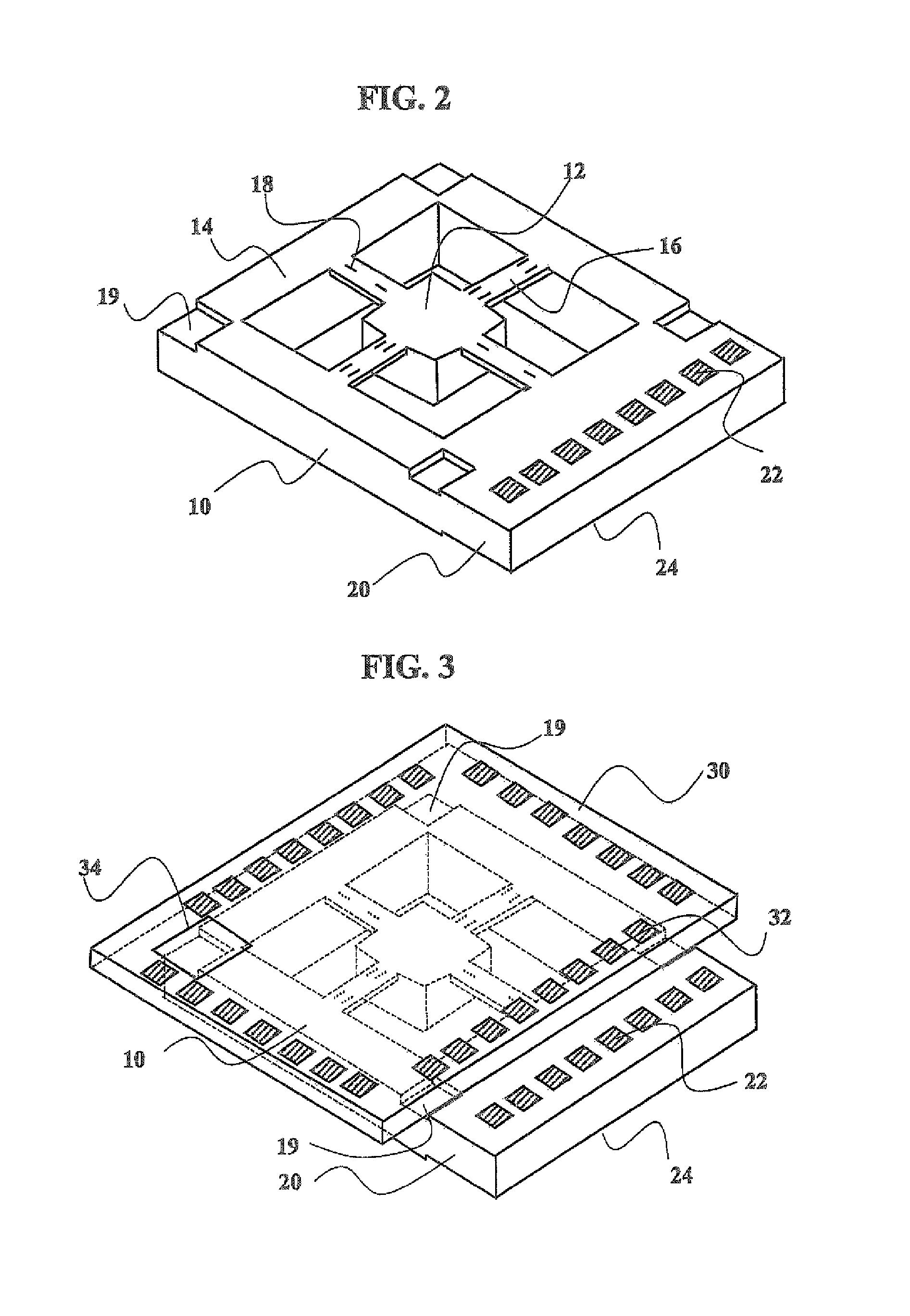
[0048]An acceleration sensor device of EXAMPLE 1 according to the present invention will be described with FIG. 1 to FIG. 5. FIG. 1 is an exploded perspective view of the acceleration sensor device of EXAMPLE 1; FIG. 2 is a perspective view showing an acceleration sensor chip used in the acceleration sensor device of EXAMPLE 1; FIG. 3 is a perspective view of the acceleration sensor chip with an upper regulation plate mounted thereon; FIG. 4 is a cross-sectional view taken along a line IV-IV of FIG. 1; and FIG. 5 is a plan view showing the acceleration sensor device of FIG. 1 with a lid removed. In the acceleration sensor device 100 of EXAMPLE 1, the upper regulation plate 30 with its circuit mounting surface on the top is bonded to the top surface of the acceleration sensor chip 10 by mixed and kneaded adhesive 36 containing about 10 wt % of rigid plastic balls (20 μm in diameter) and the acceleration sensor chip 10 is inserted and bonded in a protection case 40. To bond the accele...
example 2
[0066]The relationship between the offset voltage and the distance ratio was measured by using an acceleration sensor device according to the present invention, in which the size of the upper regulation plate is changed, and the ratio of the first side gap, between an inside wall of the protection case and a side of the upper regulation plate, to the second side gap, between the inside wall of the protection case and an outside wall of the support frame, is changed. Acceleration sensor devices used herein are the same as that of EXAMPLE 1 except for the sizes of the upper regulation plates. In the upper regulation plates, L of the size of 2200 μm in width×L μm in length×200 μm thickness was changed from 1900 μm up to 2800 μm. The upper regulation plate protrudes by 300 μm from the outside wall of the support frame on the side opposite to the side on which the terminal board is disposed because the upper regulation plate is bonded on the acceleration sensor chip so that on the side, ...
example 3
[0067]The relationship between a location of the temperature sensor disposed on the upper regulation plate and the offset voltage was considered. Acceleration sensor devices used herein have the constitution as described in EXAMPLE 1, and the temperature sensor 34 is disposed on the upper regulation plate corresponding to one of the locations where the upper regulation plate is bonded at the four corners of the support frame. When the center of a temperature measuring portion (size of 300 μm×300 μm) of the temperature sensor 34 was changed in a to-and-fro direction by a distance of W1 and in a right-and-left direction by a distance of W2 up to 300 μm as shown in FIG. 7 from the center of the corner 19 having a recess with the size of 180 μM×180 μm containing adhesive, the offset voltage was measured, and the distribution of the offset voltage is shown in FIG. 8. As seen from FIG. 8, when the center of the temperature measuring portion of the temperature sensor is an area within ±50 ...
PUM
 Abstract
Description
Claims
Application Information
 - R&D
- Intellectual Property
- Life Sciences
- Materials
- Tech Scout
- Unparalleled Data Quality
- Higher Quality Content
- 60% Fewer Hallucinations
Browse by: Latest US Patents, China's latest patents, Technical Efficacy Thesaurus, Application Domain, Technology Topic, Popular Technical Reports.
© 2025 PatSnap. All rights reserved.Legal|Privacy policy|Modern Slavery Act Transparency Statement|Sitemap|About US| Contact US: help@patsnap.com


