Semiconductor memory device

a memory device and semiconductor technology, applied in the field of semiconductor memory devices, can solve the problem that the static noise margin (snm) cannot be compensated, and achieve the effect of preventing erroneous operation, facilitating writing to the latch circuit, and reducing the area of the sram

Inactive Publication Date: 2010-04-13
SOCIONEXT INC
View PDF11 Cites 7 Cited by
  • Summary
  • Abstract
  • Description
  • Claims
  • Application Information

AI Technical Summary

Benefits of technology

[0008]An object of the present invention is to prevent an erroneous operation on a non-selected column even in a configuration in which one input / output circuit is provided for a plurality of columns in a memory cell array having memory cells arranged in a matrix, while expanding an operating voltage margin during writing of data of a semiconductor memory device.
[0011]With these configurations, during a write operation with respect to a selected memory cell, the contribution of the third or fourth access transistor facilitates writing to the latch circuit. Under other conditions, an erroneous operation can be prevented in a non-selected column, particularly in the case of a configuration in which a plurality of input / output circuits including a first input / output circuit are provided with respect to the memory cell array, and a plurality of columns of memory cells are connected to one input / output circuit. In other words, when a configuration is employed in which a plurality of columns of memory cells are connected to the first input / output circuit while expanding an operating voltage margin during a data write operation, the area of an SRAM can be reduced.
[0012]Therefore, according to the present invention, an erroneous operation can be prevented in a non-selected column even when a plurality of columns of memory cells are connected to one input / output circuit, while expanding an operating voltage margin during a write operation in a semiconductor memory device. Therefore, in an SRAM, a configuration can be employed in which a plurality of columns of memory cells are connected to one input / output circuit, resulting in a reduction in area.

Problems solved by technology

However, when a plurality of columns of memory cells are connected to one input / output circuit, a Static Noise Margin (SNM) cannot be compensated for on a bit line (column) that is not selected, disadvantageously leading to an erroneous operation.

Method used


Image

  • Semiconductor memory device
  • Semiconductor memory device
  • Semiconductor memory device

Examples


Embodiment Construction

[0040]Hereinafter, embodiments of the present invention will be described in detail with reference to the accompanying drawings. Note that like parts are indicated by like reference symbols and will not be repeatedly described.

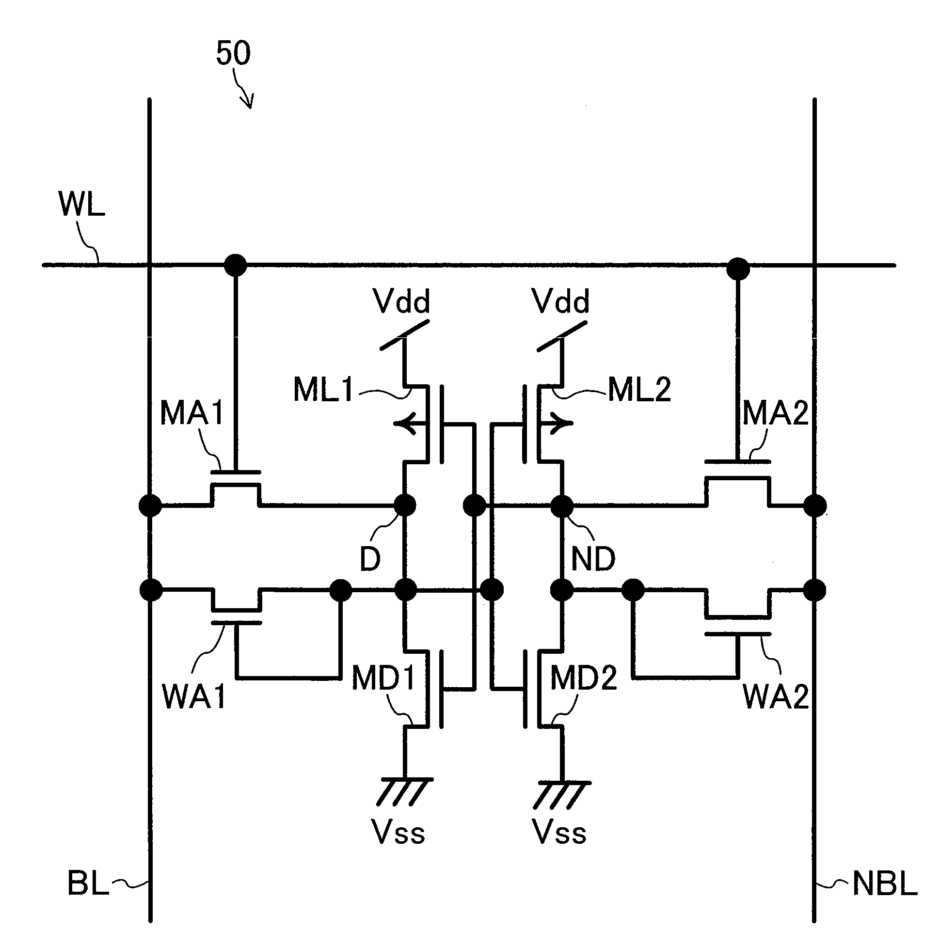
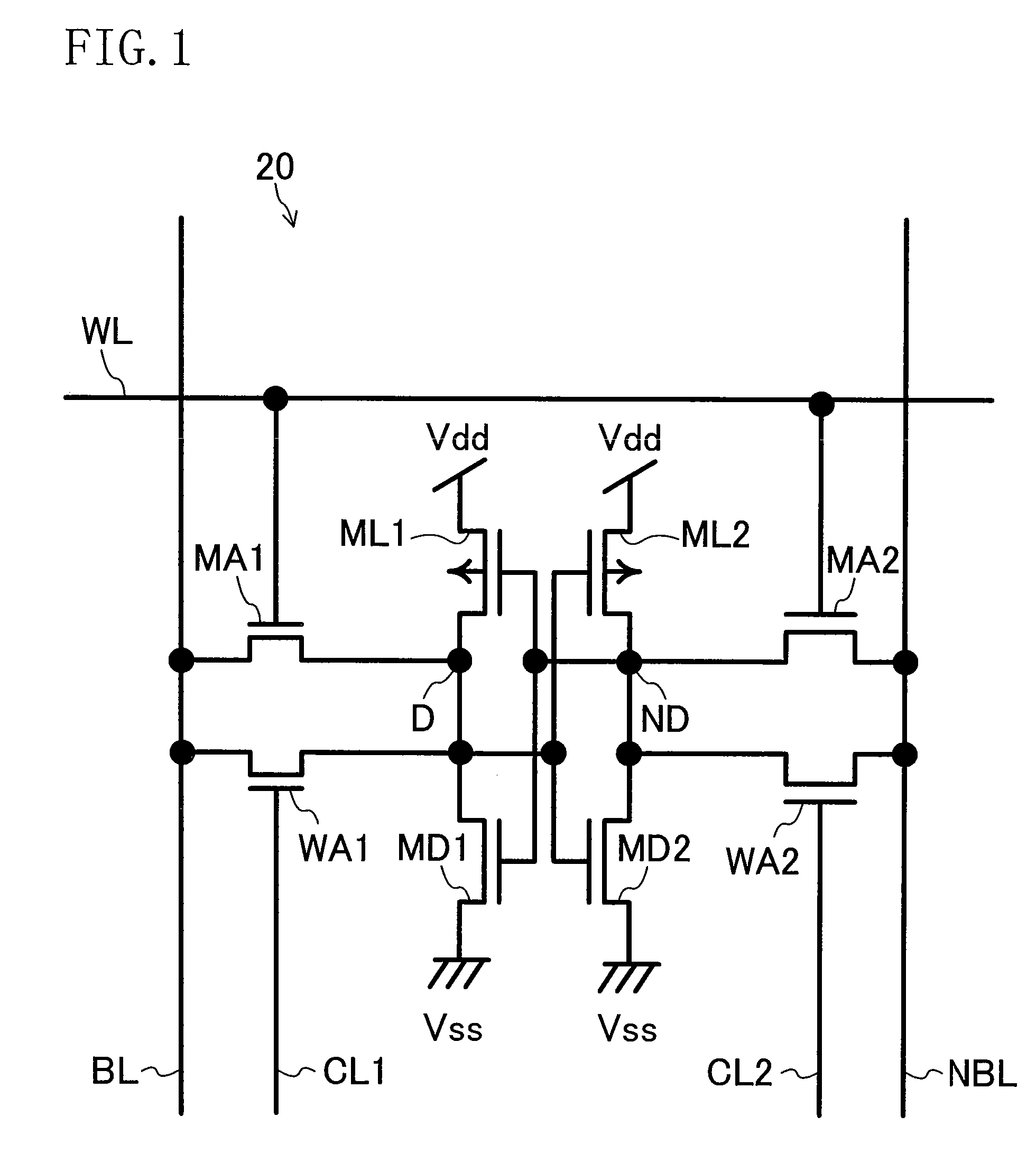
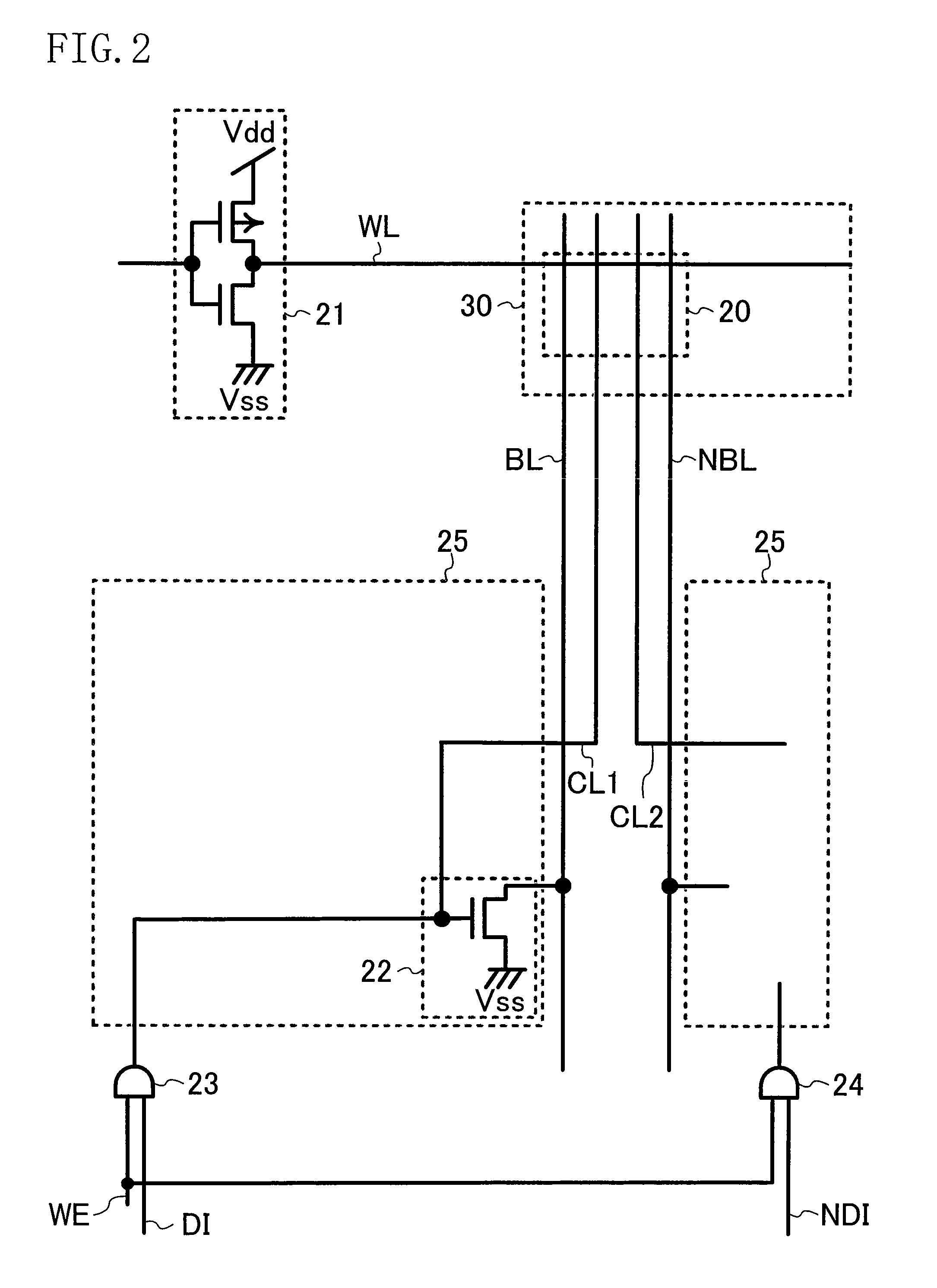
[0041]FIG. 1 shows a first exemplary configuration of a memory cell in an SRAM that is a semiconductor memory device according to an embodiment of the present invention. The memory cell 20 of FIG. 1 is a memory cell for storing complement data at first and second memory nodes D and ND, and comprises first and second load transistors ML1 and ML2, first and second drive transistors MD1 and MD2, first and second access transistors MA1 and MA2, and third and fourth access transistors (write assisting transistors) WA1 and WA2.

[0042]Specifically, the first load transistor ML1 is a P-channel MOS transistor that has a drain terminal connected to the first memory node D, a source terminal to which a power supply voltage Vdd is supplied, and a gate terminal connected to...


PUM


Abstract

In a memory cell having a first and a second load transistor, a first and a second drive transistor, and a first and a second access transistor, a third access transistor provided between a first bit line and a first memory node and having a gate terminal connected to a first column line and a fourth access transistor provided between a second bit line and a second memory node and having a gate terminal connected to a second column line, are additionally provided.

Description

BACKGROUND OF THE INVENTION[0001]1. Field of the Invention[0002]The present invention relates to a semiconductor memory device, and more particularly to a memory cell circuit and a control circuit that is used during a write operation.[0003]2. Description of the Related Art[0004]Conventionally, there is a known semiconductor memory device in which an access transistor is provided between a memory node of a memory cell and a bit line, and the access transistor is controlled using a word line (see Japanese Unexamined Patent Application Publication No. H02-094196 and U.S. Pat. No. 7,313,021).[0005]There is also a known technique in which a path between a P-channel MOS transistor of a memory cell and a memory node is interrupted so as to expand a write voltage operation range of an SRAM (Static Random Access Memory) (see U.S. Pat. No. 7,286,390).SUMMARY OF THE INVENTION[0006]In the above-described conventional techniques, when a word line selected using a row address is activated, the a...

Claims


Application Information

Patent Timeline
Patent Type & Authority Patents(United States)
IPC IPC(8): G11C11/40
CPCG11C11/419G11C11/412
Inventor MASUO, AKIRASUMITANI, NORIHIKOTSUJIMURA, KAZUKIKOIKE, TSUYOSHI
Owner SOCIONEXT INC
Why Eureka
Try Eureka