Wire grid polarizer and method of manufacturing the same
a polarizer and wire grid technology, applied in the field of wire grid polarizers, can solve the problems of increasing the overall number of elements, deteriorating brightness and excessive power consumption, and enhancing the size and weight of the device, so as to improve the extinction ratio, increase the structural reliability, and high transmittance
- Summary
- Abstract
- Description
- Claims
- Application Information
AI Technical Summary
Benefits of technology
Problems solved by technology
Method used
Image
Examples
example 1
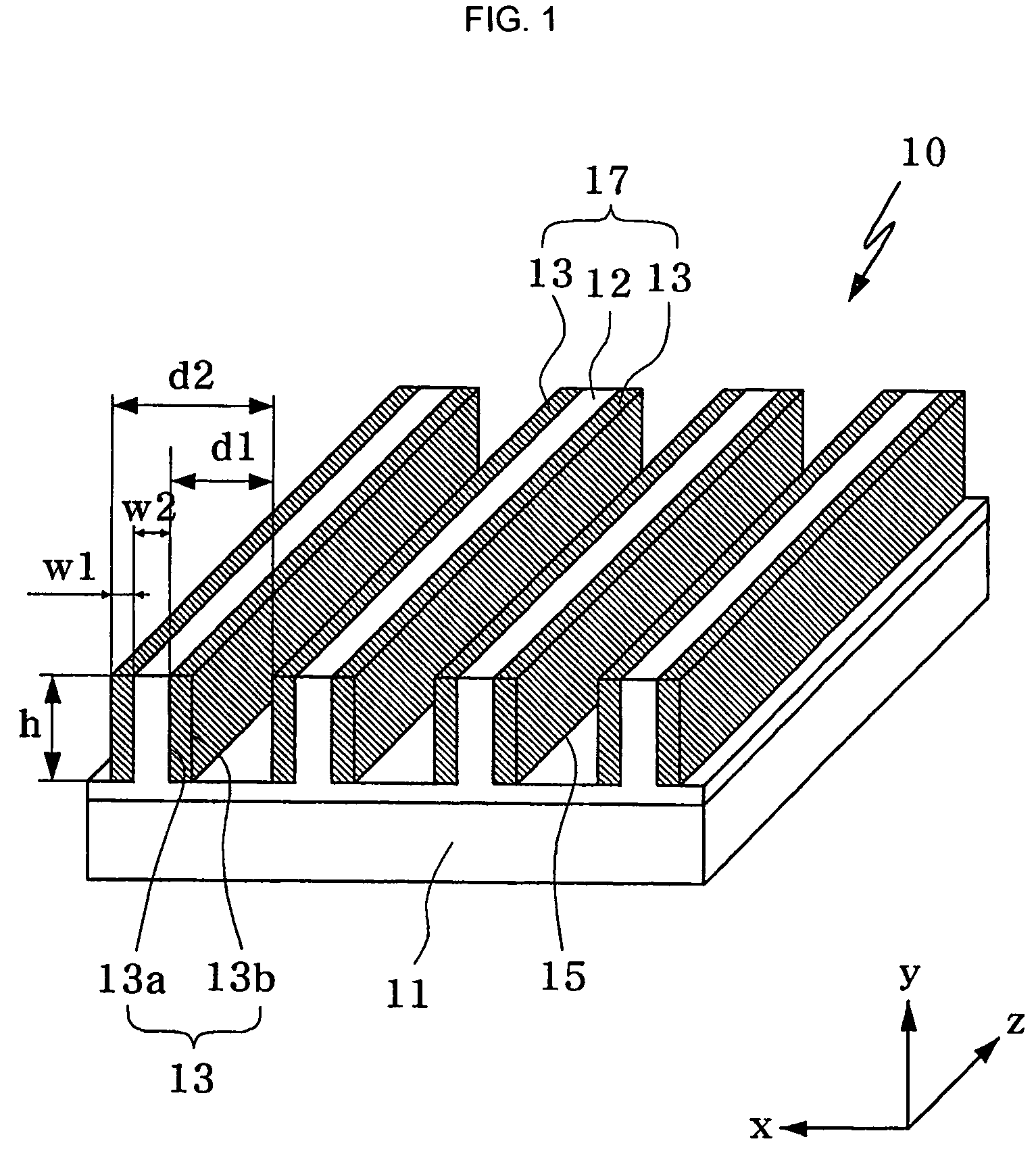
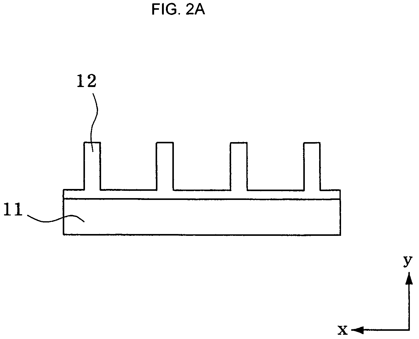
[0058]a plurality of parallel dielectric wires having a width of 49 nm, a height of 175 nm, and a pitch of 140 nm were formed on a PC film having a thickness of 100 μm by a nano-imprint lithography. The dielectric wires were formed by coating a UV curable resin, i.e., a PAK-01 having a refractive index of 1.5 (by Toyo Gosei Co. Ltd.), over the PC film by means of a wire bar, stacking a mold subjected to a release treatment on the UV curable resin, curing the resin by UV light, and releasing the mold. Distance between adjacent dielectric wires was measured to be 91 nm.
[0059]Next, an aluminum layer having a uniform thickness of 21 nm was formed over the plurality of dielectric wires by a chemical vapor deposition (CVD), i.e., upper surfaces of each dielectric wire and surfaces of each gap between adjacent dielectric wires. The CVD was used by employing a reactive gas and methylpyrrolidine-alane (MPA). That is, the PC film was heated to a temperature of 105° C. in a vacuum chamber, the...
example 2
[0062]a plurality of parallel dielectric wires having a width of 60 nm, a height of 200 nm, and a pitch of 200 nm were formed of PMMA having a refractive index of 1.5 on a glass substrate by thermal nano-imprint lithography. More specifically, the glass substrate was formed to include an anti-reflection coating, i.e., sequentially stacked three layers of titanium dioxide and one layer of silicon dioxide, on a first surface thereof. A second surface of the glass substrate, i.e., a surface opposite the anti-reflection structure, was spin-coated with a solution containing PMMA in a solvent. The solution was dried to form a PMMA layer having a thickness of 1 μm. Next, the PMMA-coated glass substrate was heated to a temperature of 150° C. to soften the PMMA layer, followed by pressing a mold to the softened PMMA layer and cooling the PMMA layer to a room temperature while keeping it in a pressed state. The mold was released to realize the dielectric wires on the glass substrate.
[0063]Nex...
example 3
[0066]a plurality of dielectric wires having a width of 50 nm, a height of 175 nm, and a pitch of 100 nm were formed in a PMMA film having a thickness of 125 μm by thermal nano-imprint lithography. Processing of the PMMA was done according to a substantially similar process described in Example 2. Next, an aluminum layer having a thickness of 300 nm was formed on the dielectric wires and in trenches therebetween by CVD. The CVD was performed by introducing MPA for 20 minutes into a vacuum chamber heated to a temperature of 105° C. and bubbling argon gas to reach an internal pressure of 30 Pa to facilitate aluminum deposition on the dielectric wires. The aluminum was deposited to form a uniform layer having a thickness of 300 nm.
[0067]Subsequently, the aluminum was etched with a sodium hydroxide (NaOH) solution having a concentration of 0.1 mol / l. More specifically, the PMMA film formed with the aluminum layer was immersed in the NaOH solution and agitated to remove the aluminum depo...
PUM
| Property | Measurement | Unit |
|---|---|---|
| aspect ratio | aaaaa | aaaaa |
| aspect ratio | aaaaa | aaaaa |
| width w2 | aaaaa | aaaaa |
Abstract
Description
Claims
Application Information
 - R&D
- Intellectual Property
- Life Sciences
- Materials
- Tech Scout
- Unparalleled Data Quality
- Higher Quality Content
- 60% Fewer Hallucinations
Browse by: Latest US Patents, China's latest patents, Technical Efficacy Thesaurus, Application Domain, Technology Topic, Popular Technical Reports.
© 2025 PatSnap. All rights reserved.Legal|Privacy policy|Modern Slavery Act Transparency Statement|Sitemap|About US| Contact US: help@patsnap.com


