Display device and electronic equipment
a technology of electronic equipment and display device, which is applied in the field of display device, can solve the problems of difficulty in realizing large-scale and high-definition displays, devices are self-luminous, etc., and achieve the effects of reducing the amount of signal potential, reducing the amount of negative feedback to the pixel capacity, and reducing the drive curren
- Summary
- Abstract
- Description
- Claims
- Application Information
AI Technical Summary
Benefits of technology
Problems solved by technology
Method used
Image
Examples
first embodiment
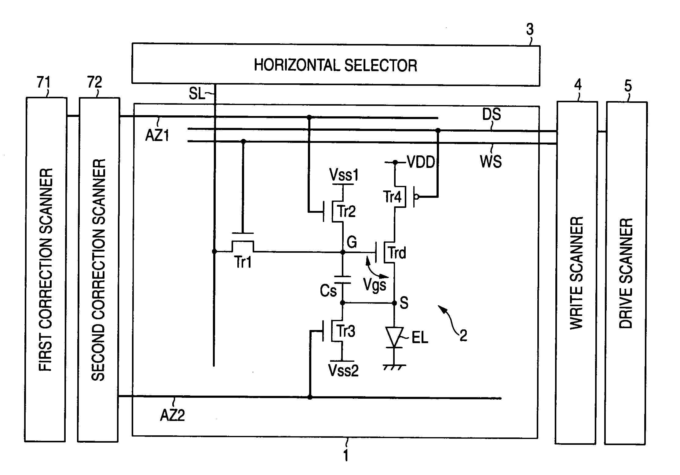
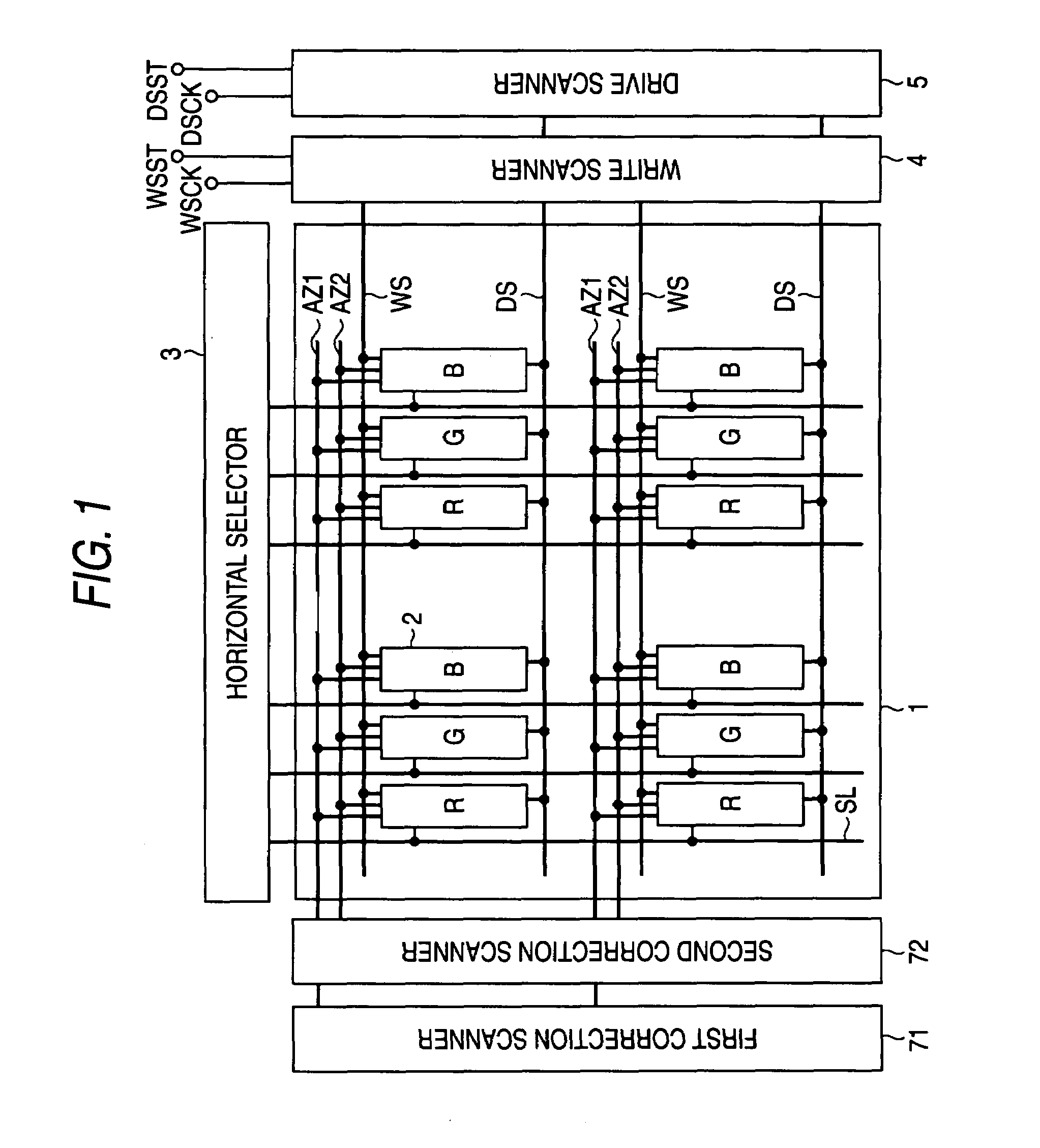
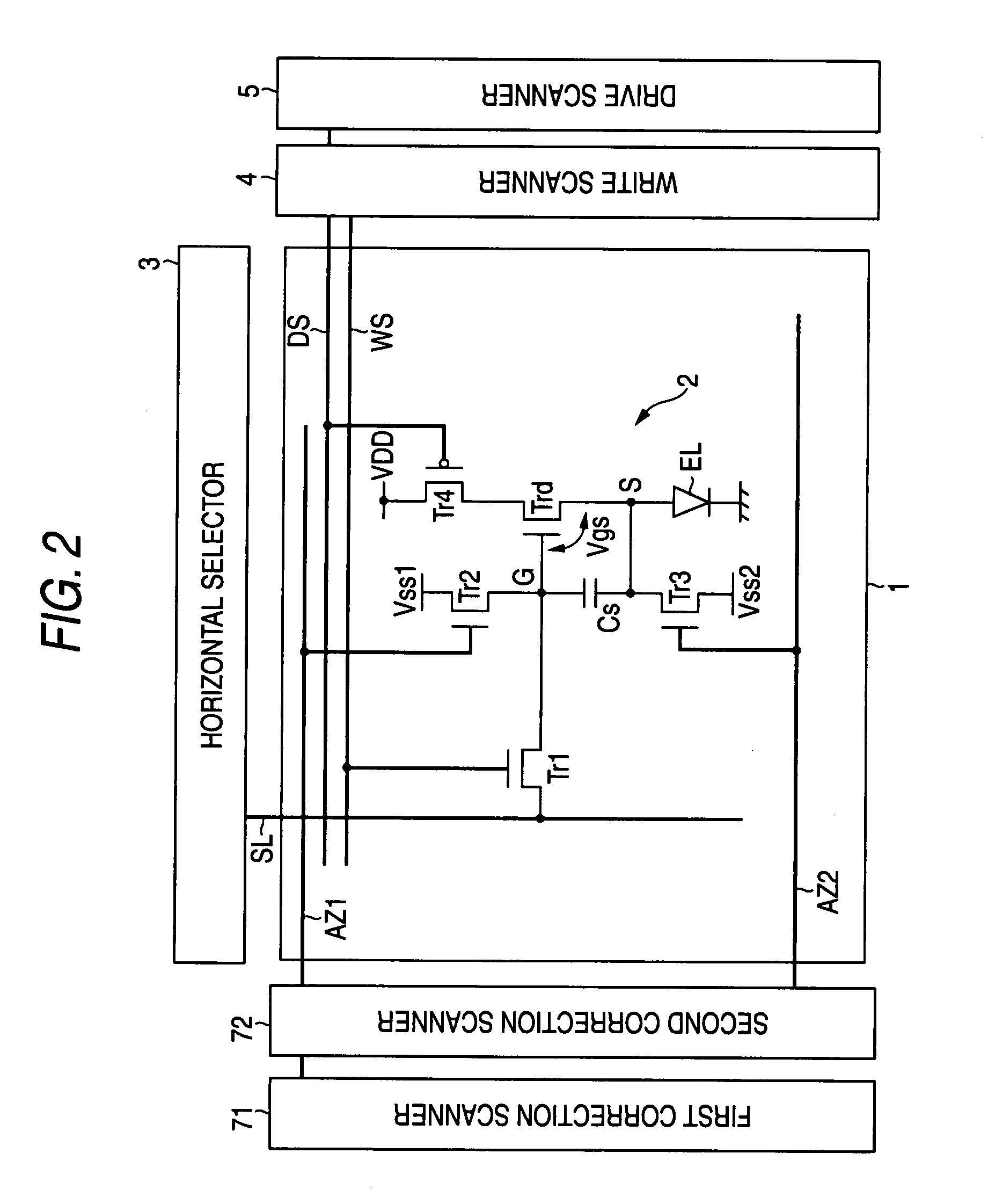
[0078]In the current flat panel market, products with higher screen brightness are in demand. Accordingly, it is necessary to shorten the mobility correction time that acts on the signal potential to be reduced. When the mobility correction time is made shorter, streaks due to uneven brightness are noticeable with a slight shift of duration. The variations in correction time are principally caused by variations in threshold voltages of the switching transistor and the sampling transistor. Accordingly, the basic concept of the invention is to make the transition waveforms of the control signal pulses applied to the gates of these transistors steeper so that, if the threshold voltages of the transistors vary, the correction time itself may not vary. FIG. 10 is a schematic circuit diagram showing the first embodiment created based on the basic concept of the invention. FIG. 10 schematically shows three stages of output units of the write scanner 4 and three columns (three lines) of the...
second embodiment
[0085]FIGS. 13A to 13C are schematic diagrams showing a display device of the second embodiment according to the invention. FIG. 13A shows a pixel configuration, FIG. 13B shows waveforms of control signals WS and DS, and FIG. 13C shows a gate pattern of an output buffer of the write scanner. As shown in FIG. 13A, the embodiment uses a P-channel transistor as the sampling transistor Tr1. Accordingly, as shown in FIG. 13B, the determining waveform of the control signal WS applied to the sampling transistor Tr1 is not the falling waveform shown in FIG. 12, but a rising waveform. Therefore, as shown in FIG. 13C, in the output buffer of the write scanner that supplies the control signal WS, the P-channel transistor is a superior switching element that principally forms the rising waveform of the control signal WS, and the N-channel transistor is an inferior switching element on the contrary. In the embodiment, in order to make the determining waveform steeper, the channel width of the P-...
third embodiment
[0086]FIGS. 14A to 14C are schematic diagrams showing a display device of the third embodiment according to the invention. As shown in FIG. 14A, the embodiment uses an N-channel transistor as the switching transistor Tr4. Accordingly, as shown in FIG. 14B, the rising waveform of the control signal DS is the determining waveform that determines the start of the mobility correction time. As shown in FIG. 14C, in the output buffer of the drive scanner 5 that supplies the control signal DS, the channel width of the P-channel transistor at the superior switching element side that forms the determining waveform is made wider than the channel width of the N-channel transistor at the inferior switching element side. Thereby, the rising waveform of the control signal DS can be made steeper than the falling waveform.
PUM
 Abstract
Description
Claims
Application Information
 - R&D
- Intellectual Property
- Life Sciences
- Materials
- Tech Scout
- Unparalleled Data Quality
- Higher Quality Content
- 60% Fewer Hallucinations
Browse by: Latest US Patents, China's latest patents, Technical Efficacy Thesaurus, Application Domain, Technology Topic, Popular Technical Reports.
© 2025 PatSnap. All rights reserved.Legal|Privacy policy|Modern Slavery Act Transparency Statement|Sitemap|About US| Contact US: help@patsnap.com


