Method and apparatus for blocking light to peripheral circuitry of an imager device
a technology of imager device and peripheral circuit, which is applied in the direction of electrical equipment, semiconductor devices, radio frequency controlled devices, etc., can solve the problems of degrading imager device performance and interfering with proper image capture, and achieve the effect of reducing or eliminating the amount of radiant energy striking
- Summary
- Abstract
- Description
- Claims
- Application Information
AI Technical Summary
Benefits of technology
Problems solved by technology
Method used
Image

Examples
second embodiment
[0040]FIG. 7 illustrates a partial cross-sectional view of an integrated circuit 200 constructed in accordance with the invention in which first and second frames 216, 218 are formed as mesas of a color filter array 217. The first and second frames 216, 218 are formed by providing a color filter array precursor layer, and forming trenches in the precursor layer, thereby creating corresponding mesas that form the first and second frames 216, 218. The planarization layer 191 is selectively formed over the color filter array 217 such that the planarization layer 191 is formed within the trenches formed in the color filter array precursor layer (i.e., not over the mesas that form the first and second frames 216, 218). A microlens array 141 is formed over the planarization layer 191. The material layer 124 is formed over the first and second frames 216, 218, and in between the first and second frame 116, 118, in a substantially similar fashion as discussed above with respect to FIGS. 5 a...
third embodiment
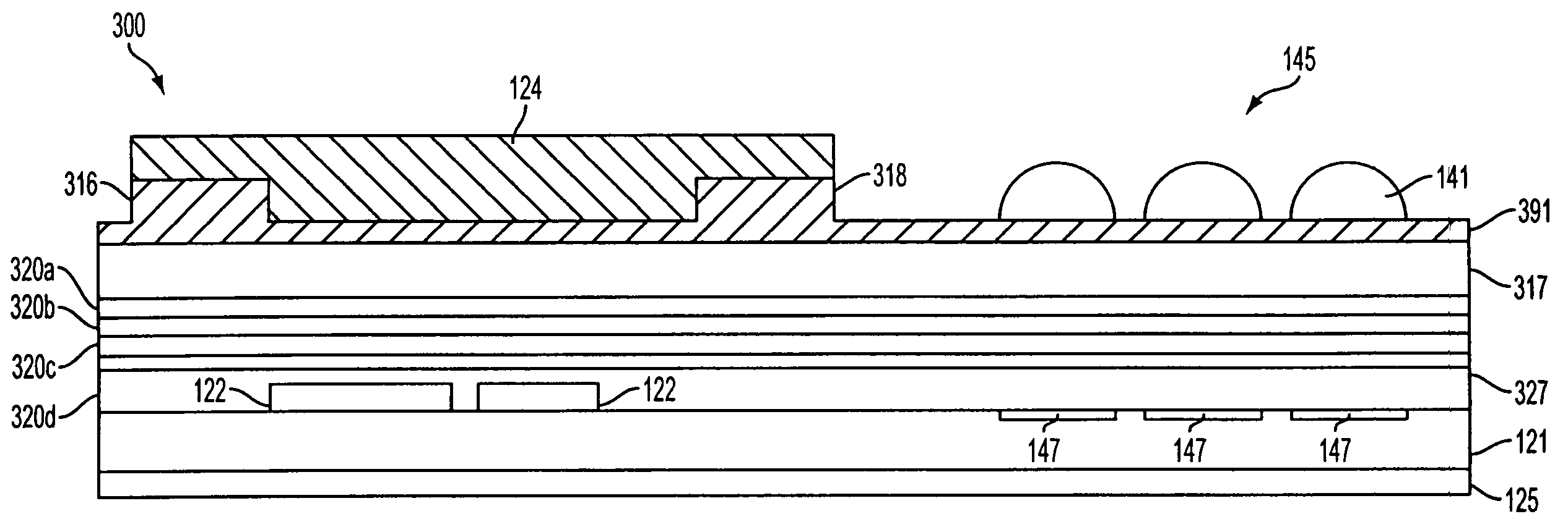
[0041]FIG. 8 illustrates a partial cross-sectional view of an integrated circuit 300 constructed in accordance with the invention in which first and second frames 316, 318 are formed as mesas of a planarization layer 391. The first and second frames 316, 318 could be formed by forming a planarization precursor layer, and etching trenches within the planarization precursor layer, thereby creating corresponding mesas that form the first and second frames 316, 318. FIG. 8 illustrates a color filter array 317 formed beneath the planarization layer 391. A microlens array 141 is subsequently formed over the planarization layer 391. The material layer 124 is formed in a substantially similar fashion as discussed above with respect to FIGS. 5 and 6.
[0042]It should be noted that although FIGS. 6-8 illustrate first and second frames 116, 118 (FIG. 6), 216, 218 (FIG. 7), 316, 318 (FIG. 8) formed as mesas of microlens material, color filter array material, and planarization layer material, resp...
fifth embodiment
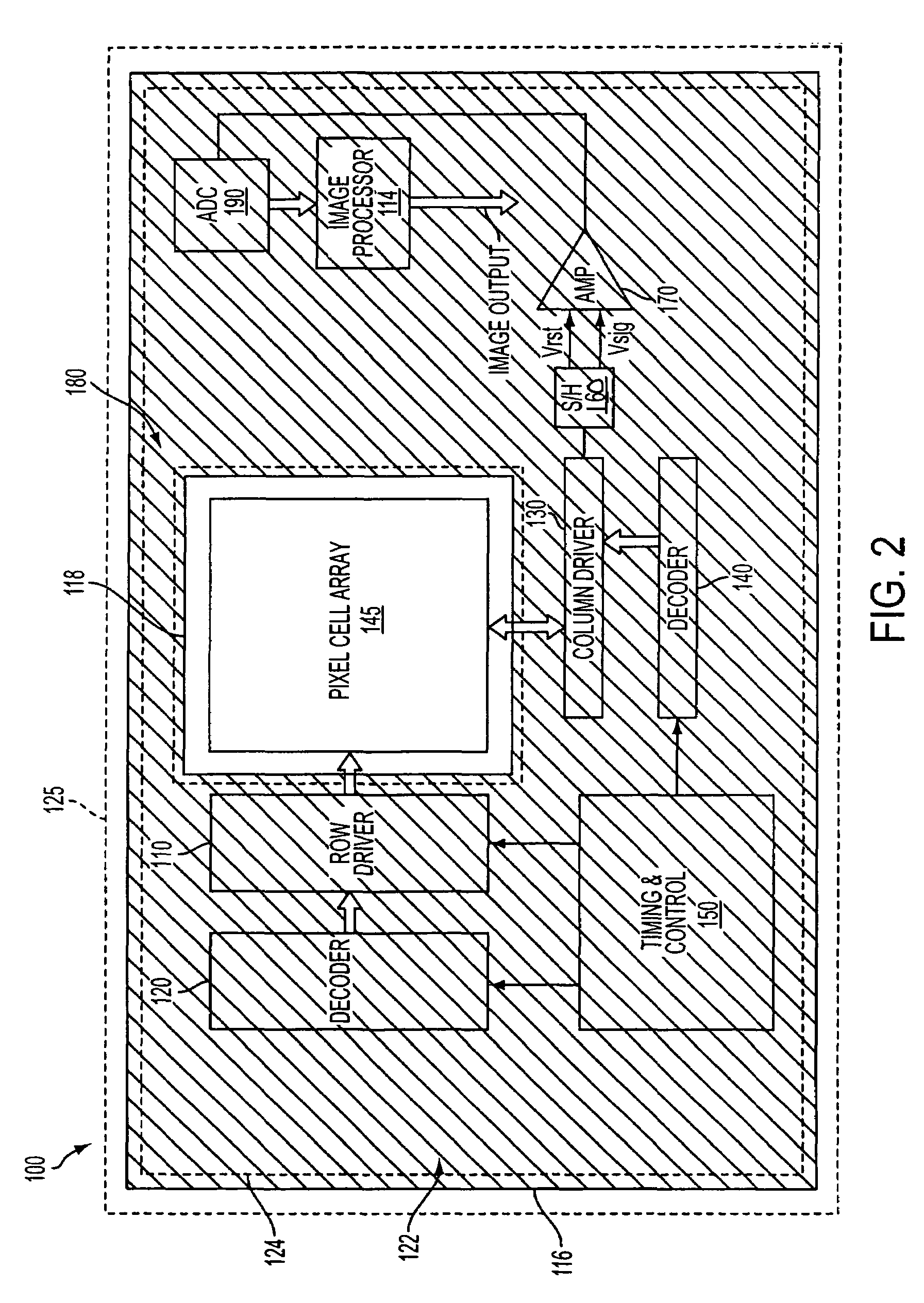
[0045]FIG. 10 illustrates an integrated circuit 500 constructed in accordance with the invention. The integrated circuit 500 includes an imager device 580 formed on a die 525. The imager device 580 includes components that comprise peripheral circuitry 522. Each component of the peripheral circuitry 522 has a respective frame forming a perimeter around the component. The FIG. 10 integrated circuit 500 includes a row driver 510, column driver 530, row decoder 520, column decoder 540, timing and control circuit 550, analog-to-digital converter 590, sample and hold circuit 560, differential amplifier 570, and an image processor 514. Accordingly, the integrated circuit 500 includes a row driver frame 511, column driver frame 531, row decoder frame 521, column decoder frame 541, timing and control circuit frame 551, analog to digital converter frame 591, sample and hold circuit frame 561, amplifier frame 571, and an image processor frame 581. A material layer 524 is formed over each comp...
PUM
 Abstract
Description
Claims
Application Information
 - R&D
- Intellectual Property
- Life Sciences
- Materials
- Tech Scout
- Unparalleled Data Quality
- Higher Quality Content
- 60% Fewer Hallucinations
Browse by: Latest US Patents, China's latest patents, Technical Efficacy Thesaurus, Application Domain, Technology Topic, Popular Technical Reports.
© 2025 PatSnap. All rights reserved.Legal|Privacy policy|Modern Slavery Act Transparency Statement|Sitemap|About US| Contact US: help@patsnap.com