Pattern transfer mask, focus variation measuring method and apparatus, and semiconductor device manufacturing method
a technology of focus variation and mask, applied in the field of pattern transfer mask, focus variation measuring method and apparatus, semiconductor device manufacturing method, etc., can solve the problems of deteriorating size uniformity, focus error, and exposure errors of aligners
- Summary
- Abstract
- Description
- Claims
- Application Information
AI Technical Summary
Benefits of technology
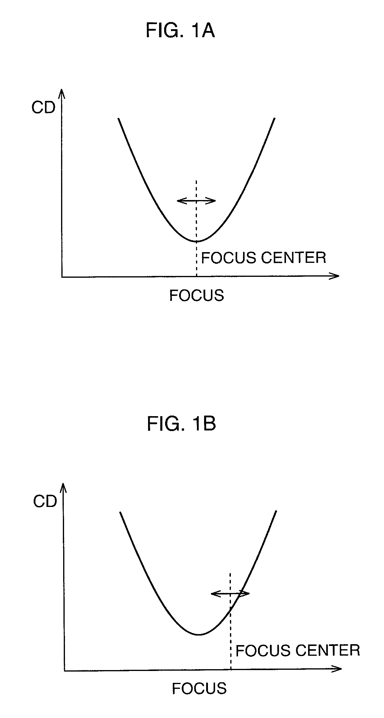
Problems solved by technology
Method used
Image


Examples
modified examples
[0083]Hereinafter, various modified examples according to the present embodiment will be explained.
[0084]The modified examples differ from the present embodiment in a structure of a reticle. Note that the same reference numerals and symbols are used to designate substantially the same constituent elements as the present embodiment, and detailed description thereof will be omitted.
modified example 1
Structure of Reticle
[0085]FIG. 9 is a schematic sectional view showing a main structure of a reticle according to a modified example 1 of the present embodiment.
[0086]A reticle of the example has a main pattern 11 and a monitor pattern 31 formed by patterning a light-shielding film 4 formed on a quartz substrate 3. Here, the main pattern 11 and the monitor pattern 31 are formed with mutually different height values. Concretely, the main pattern 11 and the monitor pattern 31 have different thicknesses of the light-shielding film 4, in which the monitor pattern 31 is formed thinner compared to the main pattern 11. For instance, the main pattern 11 and the monitor pattern 31 are respectively formed to have about 100 nm and 50 nm in thickness, so that the difference in thickness of both patterns is set to be about 50 nm.
[0087][Manufacturing Method of Reticle]
[0088]An example of a manufacturing method of the above-described reticle will be explained. FIG. 10A to FIG. 10C are schematic se...
modified example 2
Structure of Reticle
[0093]FIG. 11 is a schematic sectional view showing a main structure of a reticle according to a modified example 2 of the present embodiment.
[0094]A reticle of the example has a main pattern 11 and a monitor pattern 41 formed by patterning a quartz substrate 3 and a light-shielding film 4 formed on the quartz substrate 3. Here, the main pattern 11 and the monitor pattern 41 are formed with mutually different height values. Concretely, the main pattern 11 and the monitor pattern 41 have the same thickness of the light-shielding film 4, but, in the monitor pattern 41, not only the light-shielding film 4 but also the quartz substrate 3 are processed together so that the monitor pattern 41 is formed higher (deeper) compared to the main pattern 11. For instance, the main pattern 11 and the monitor pattern 41 are respectively formed to have about 50 nm and 100 nm in height, so that the difference in height (depth) of both patterns is set to be about 50 nm.
[0095][Manuf...
PUM
| Property | Measurement | Unit |
|---|---|---|
| thicknesses | aaaaa | aaaaa |
| thicknesses | aaaaa | aaaaa |
| thicknesses | aaaaa | aaaaa |
Abstract
Description
Claims
Application Information
 - R&D Engineer
- R&D Manager
- IP Professional
- Industry Leading Data Capabilities
- Powerful AI technology
- Patent DNA Extraction
Browse by: Latest US Patents, China's latest patents, Technical Efficacy Thesaurus, Application Domain, Technology Topic.
© 2024 PatSnap. All rights reserved.Legal|Privacy policy|Modern Slavery Act Transparency Statement|Sitemap