Selectable JTAG or trace access with data store and output
What is Al technical title?
Al technical title is built by PatSnap Al team. It summarizes the technical point description of the patent document.
a data store and data access technology, applied in the field of jtag or trace access with data store and output, can solve the problem of limited data input/output bandwidth of the jtag bus
Active Publication Date: 2009-08-04
TEXAS INSTR INC
View PDF6 Cites 54 Cited by
Summary
Abstract
Description
Claims
Application Information
AI Technical Summary
This helps you quickly interpret patents by identifying the three key elements:
Problems solved by technology
Method used
Benefits of technology
Problems solved by technology
For example, the data input / output bandwidth of the JTAG bus is limited to the amount of data that can flow between the JTAG controller and IC over the single TDO to TDI signal wire connections.
Method used
Image
Click on the blue label to locate the original text in one second.
Reading with bidirectional positioning of images and text.
Examples
case b
[0190] If OUT=Low & TDO=High, Then DIO=Mid, TDI=High, & IN=Low
case c
[0191] If OUT=High & TDO=Low, Then DIO=Mid, TDI=Low, & IN=High
case d
[0192] If OUT=High & TDO=High, Then DIO=High, TDI=High, & IN=High
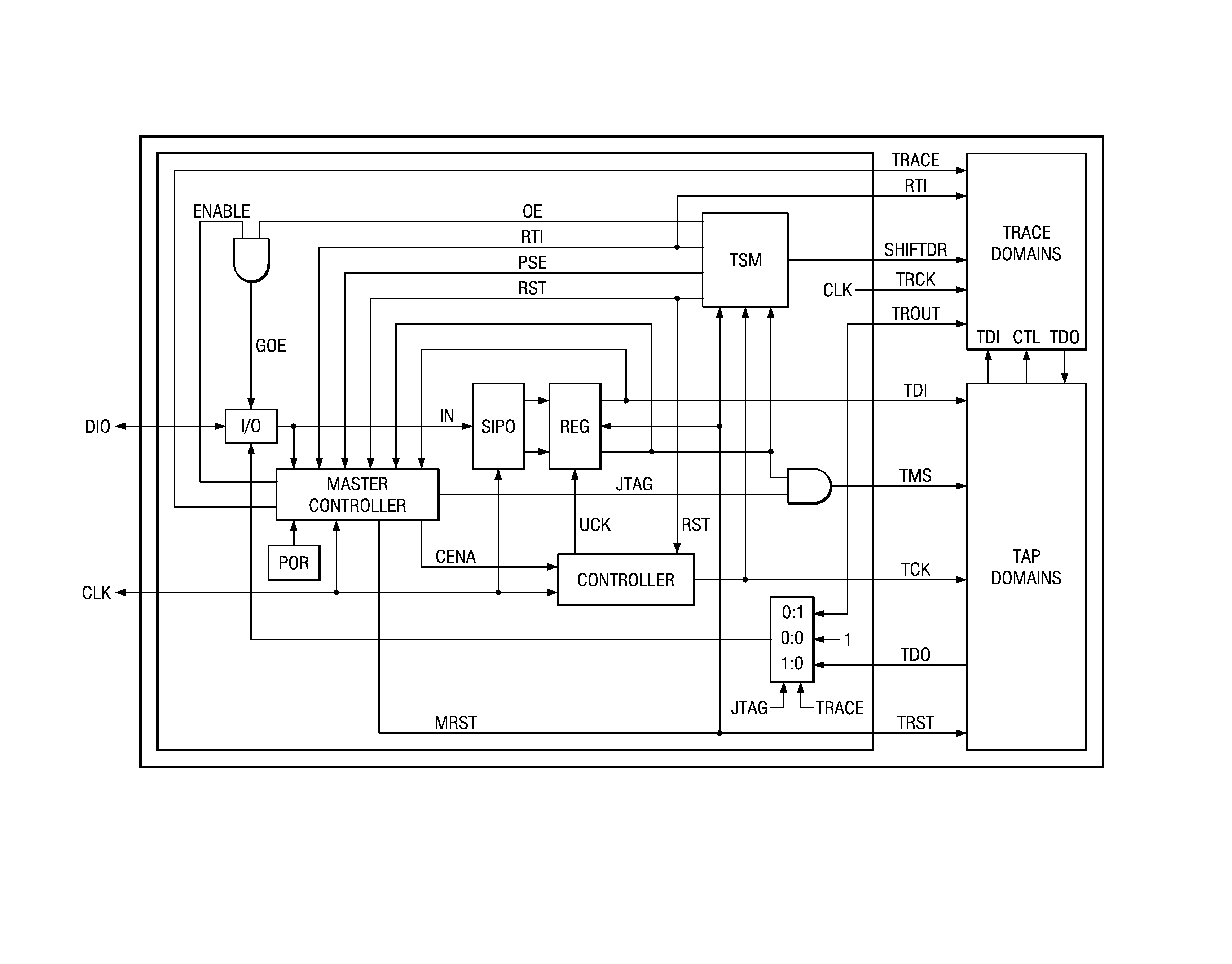
[0193]Case A shows PSC 302 driving OUT low and Tap Domains 104 driving TDO low. As seen in Case A of FIG. 12, with lows being output from both buffers 1104 and 1110 only a small amount of current flows on the DIO signal wire. This small current flow does not develop a significant voltage drop across resistors 1106 and 1112. Thus the DIO signal input to the input circuits 1102 and 1108 will be easily detectable as being a low signal input. In response to this OUT and TDO output condition the DIO signal is driven low. With OUT and DIO low, the input circuit 1102 inputs a low on the TDI input to JTAG controller 100. With TDO and DIO low, the input circuit 1108 inputs a low on the IN input to SPC 306.
[0194]Case B shows PSC 302 driving OUT low and Tap Domains 104 driving TDO high. As seen in Case B of FIG. 12, with a low being output from buffer 1104 and a high being output from buffer 1110 a larger current flows between th...
PUM
Abstract
An addressable interface selectively enables JTAG TAP domain operations or Trace domain operations within an IC. After being enabled, the TAP receives TMS and TDI input from a single data pin. After being enabled, the Trace domain acquires data from a functioning circuit within the IC in response to a first clock and outputs the acquired data from the IC in response to a second clock. An addressable two pin interface loads and updates instructions and data to a TAP domain within the IC. The instruction or data update operations in multiple ICs occur simultaneously. A process transmits data from an addressed target device to a controller using data frames, each data frame comprising a header bit and data bits. The logic level of the header bit is used to start, continue, and stop the data transmission to the controller. A data and clock signal interface between a controller and multiple target devices provides for each target device to be individually addressed and commanded to perform a JTAG or Trace operation. Trace circuitry within an IC can operate autonomously to store and output functional data occurring in the IC. The store and output operations of the trace circuitry are transparent to the functional operation of the IC. An auto-addressing RAM memory stores input data at an input address generated in response to an input clock, and outputs stored data from an output address generated in response to an output clock.
Description
CROSS-REFERENCE TO RELATED APPLICATIONS[0001]This disclosure is related to the following pending US patent applications and patents: Ser. No. 11 / 938,923 “Reduced Signaling Interface Method and Apparatus”; Ser. No. 11 / 293,061 “Selectable Pin Count JTAG”; Ser. No. 11 / 258,315 “Two Pin Serial Bus Communication Interface and Process”; Ser. No. 09 / 458,313 “TAP With Scannable Control Circuit For Selecting First Test”; Ser. No. 11 / 292,597, “Multiple Test Access Port Protocols Sharing Common Signals”; U.S. Pat. No. 5,483,518, issued Jan. 9, 1996, titled “Addressable Shadow Port and Protocol”; Seer. No. 11 / 370,017 “Optimized JTAG Interface”; U.S. Pat. No. 5,001,713, issued Mar. 19, 1991, titled “Event Qualified Testing Architecture for Integrated Circuits; U.S. Pat. No. 5,103,450, issued Apr. 7, 1992, titled “Event Qualified Testing Protocols for Integrated Circuits”; U.S. Pat. No. 5,623,500, issued Apr. 22, 1997, titled “Event Qualified Test Architecture”; U.S. Pat. No. 5,353, issued Oct. 4,...
Claims
Application Information
Patent Timeline
Application Date:The date an application was filed.
Publication Date:The date a patent or application was officially published.
First Publication Date:The earliest publication date of a patent with the same application number.
Issue Date:Publication date of the patent grant document.
PCT Entry Date:The Entry date of PCT National Phase.
Estimated Expiry Date:The statutory expiry date of a patent right according to the Patent Law, and it is the longest term of protection that the patent right can achieve without the termination of the patent right due to other reasons(Term extension factor has been taken into account ).
Invalid Date:Actual expiry date is based on effective date or publication date of legal transaction data of invalid patent.