
EMC gasket filler and method

Inactive Publication Date: 2009-02-17
IBM CORP
View PDF18 Cites 42 Cited by
  • Summary
  • Abstract
  • Description
  • Claims
  • Application Information

AI Technical Summary

Problems solved by technology

Unfortunately, despite many of the advantages associated with this industry goal, there are several important challenges that have to be overcome by the designers of these systems.
A particularly challenging area for the designers of these systems is the issue of resolving electromagnetic interference (EMI).
As the number of components are increased, electromagnetic leakage concerns continue to grow.
If unresolved, EMI can affect system performance, data integrity and speed.
Obviously, in larger system environments, the increased number of components that are stored in close proximity to one another, greatly increases the EMI concerns.
This is because while such effects can be tolerated when few devices and components exist, the increasing number of components and devices can seriously impact system integrity and performance.
This problem is further exacerbated by the improvement in semiconductor devices which allow them to operate at higher speeds, generally causing emission in higher frequency bands where interference is more likely to occur.
However, a common problem with such gaskets are that they do not fully contain EMC emissions when the slot is not populated by an active card assembly.
Since the conventional style EMC gasket filler does not fully contain EMC emissions, it doesn't provide suitable EMI protection and may even pose a threat for a potential short.

Method used


Image

  • EMC gasket filler and method
  • EMC gasket filler and method
  • EMC gasket filler and method

Examples


Embodiment Construction

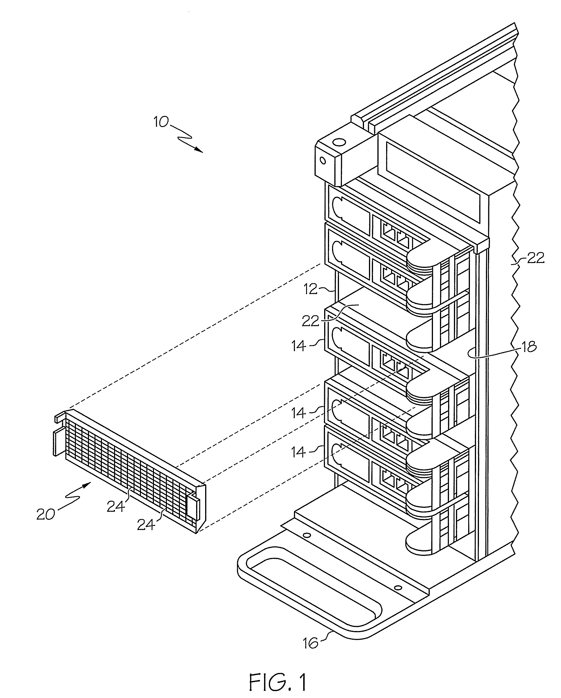
[0020]Referring generally to the figures, an electrical enclosure 10 having a plurality of slots 12 for mounting a card assembly 14 into a computer system is shown, in accordance with an embodiment of the invention. electrical enclosure 10 preferably provides structural support to the card assembly 14 so as to allow for the easy insertion and removal of the card assembly 14 from a computer system, as well as thermal and electrical isolation from other card assemblies and components within the computer system. It will also be noted that although the present invention will be described with reference to providing an EMC filler gasket with respect to the electrical enclosure 10 and a computer system, that the present invention may be employed with other devices in conjunction with an electrical enclosure.

[0021]The electrical enclosure 10 is disposed onto a computer system main board or main printed circuit board (PCB) (not shown). The electrical enclosure 10 is preferably slidably enga...


PUM


Abstract

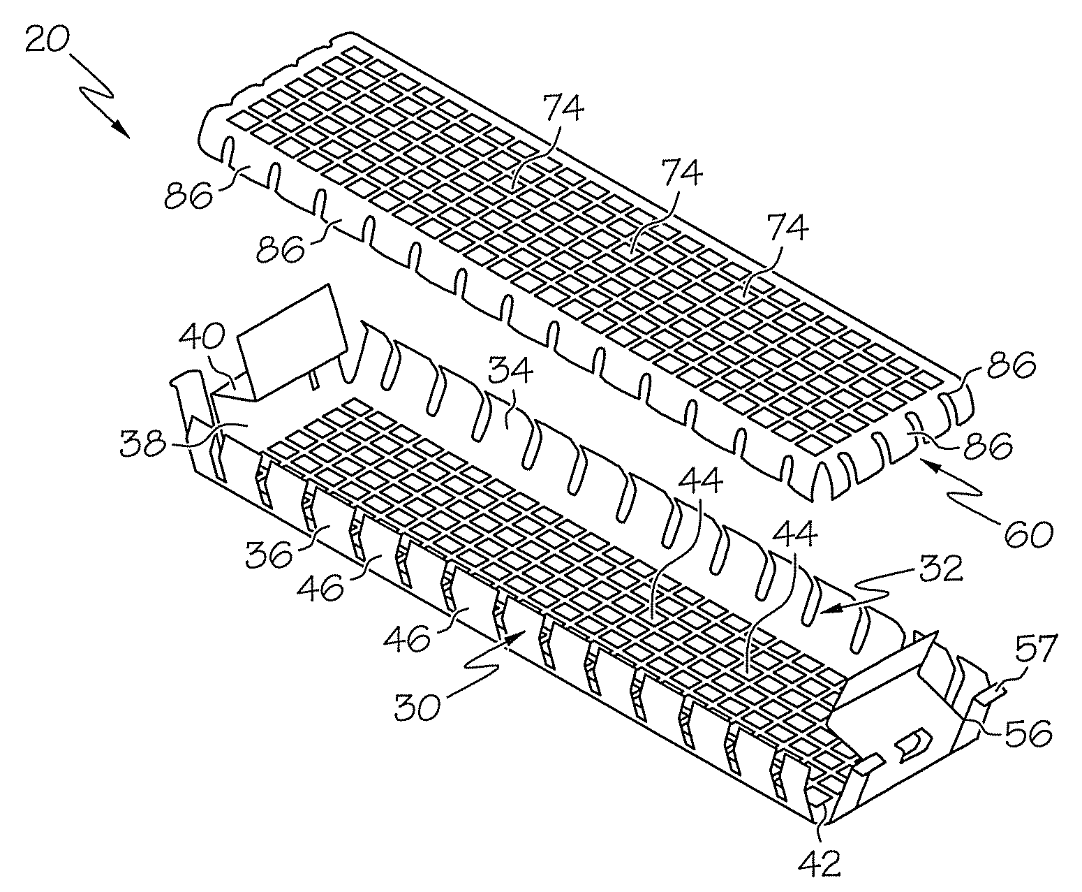
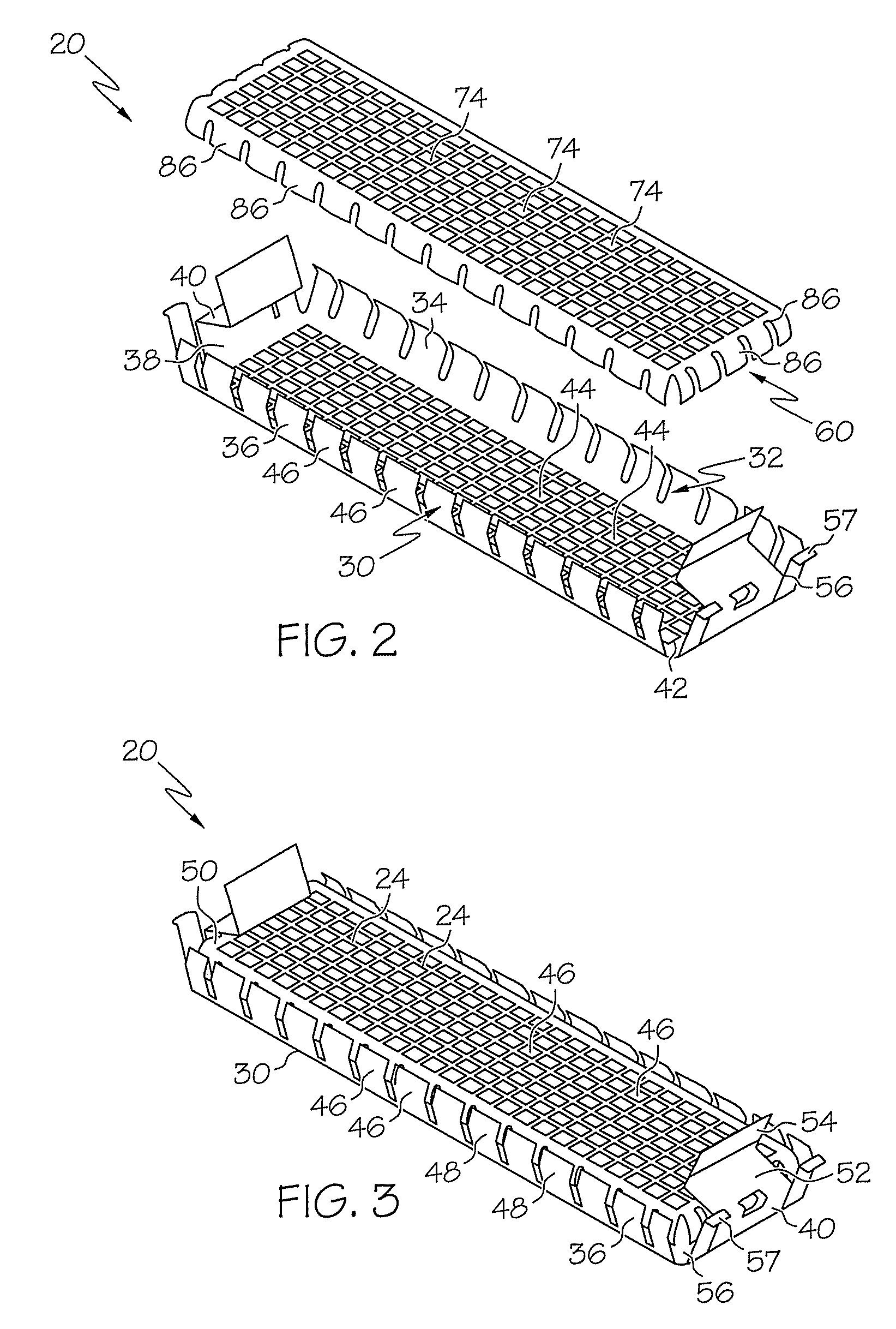
An electromagnetic gasket includes a first conductive shell having a pair of first side walls and a pair of first end walls extending from a first bottom wall defining a first opening, the pair of first side walls each having at least one first outward bias positioned thereon, the pair of first end walls each having a first tab extending therefrom, and the first bottom wall having an array of first openings and a pair of apertures; and a second conductive shell having a pair of second side walls and a pair of second end walls extending from a second bottom wall defining a second opening, the pair of second side walls and pair of second end walls each having at least one second outward bias positioned thereon, and the second bottom wall having an array of second openings. The First outward bias is configured to electrically connect to an inner surface defining an empty slot of an electrical enclosure. The second outward bias electrically connects the second conductive shell to first conductive shell when the second conductive shell is disposed within the first opening defined by the first conductive shell.

Description

BACKGROUND OF THE INVENTION[0001]1. Field of the Invention[0002]The present invention relates to an electromagnetic compatibility (EMC) sealing apparatus and related method; and more particularly to an EMC sealing apparatus and method for an empty slot of an electrical enclosure used in computing system environments.[0003]2. Description of Background[0004]It is an industry goal to continuously increase the number of electronic components inside an electronic device. This goal is driven by several key and important reasons. The first and more obvious one is for the convenience of compactness. Compactness allows for selective fabrication of smaller and lighter devices that are more attractive to the consumer. Some of the reasons for such appeal stem from a desire for easier transportation, shipping, installation and storage of such devices. In other instances, when compactness per se is not a driving factor, providing the same number of devices in only a fraction of available footprin...

Claims


Application Information

Patent Timeline
IPC IPC(8): H05K9/00H02B1/06
CPCH05K9/0016
Inventor PEETS, MICHAEL T.RYBAK, ANDREW
Owner IBM CORP
Learn More