Apparatus and method for optical amplification in indirect-gap semiconductors

a technology of indirect gap semiconductors and optical amplification, applied in the field of optical amplification in semiconductors, can solve the problem that silicon is not considered a favorable candidate for these applications

Active Publication Date: 2009-02-03
RUSCHIN SHLOMO +1
View PDF3 Cites 2 Cited by
  • Summary
  • Abstract
  • Description
  • Claims
  • Application Information

AI Technical Summary

Problems solved by technology

At present, Silicon is not considered a favorable candidate for these applications, by virtue of indirect band gap structure.

Method used


Image

  • Apparatus and method for optical amplification in indirect-gap semiconductors
  • Apparatus and method for optical amplification in indirect-gap semiconductors
  • Apparatus and method for optical amplification in indirect-gap semiconductors

Examples


Embodiment Construction

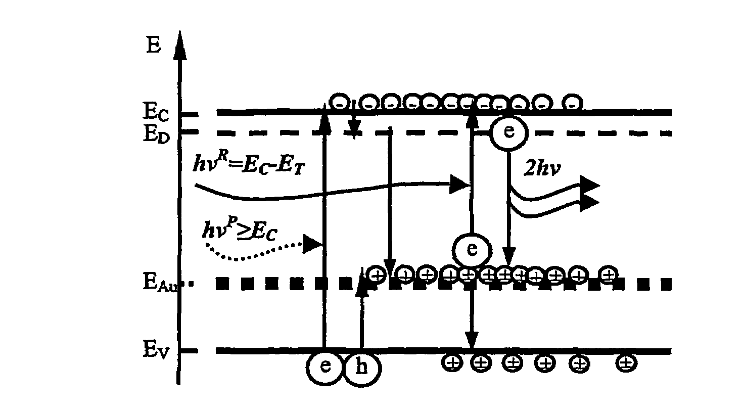
[0049]The present invention relates to methods and corresponding apparatus for achieving optical amplification in semiconductors, particularly indirect band-gap semiconductors, and most particularly in silicon. A first aspect of the invention relates to the use of certain doping elements to provide inter-band-gap energy levels in combination with optical and / or current-injection pumping. The doping element, preferably a noble metal and most preferably Gold, is chosen to provide an energy level which enables an energy transition corresponding to a photon of wavelength equal to the signal wavelength to be amplified. The energy transition may be finely “adjusted” by use of standard doping techniques (such as n-type or p-type doping) to alter the conduction and valence band energy levels and thereby also the magnitude of the energy transition. A second aspect of the invention relates to the use of a non-homogeneous heat distribution which has been found to lead to optical amplification ...


PUM


Abstract

Methods and corresponding apparatus for optical amplification in semiconductors, particularly indirect band-gap semiconductors, and most particularly in silicon. A first aspect of the invention employs certain doping elements to provide inter-band-gap energy levels in combination with optical or current-injection pumping—The doping element, preferably a noble metal and most preferably Gold, is chosen to provide an energy level which enables an energy transition corresponding to a photon of wavelength equal to the signal wavelength to be amplified. The energy transition may be finely “adjusted” by use of standard doping techniques (such as n-type or p-type doping) to alter the conduction and valence band energy levels and thereby also the magnitude of the energy transition. A second aspect of the invention relates to the use of a non-homogeneous heat distribution which has been found to lead to optical amplification effects.

Description

FIELD AND BACKGROUND OF THE INVENTION[0001]The present invention relates to optical amplification and, in particular, it concerns optical amplification in semiconductors, particularly silicon, by optical pumping and / or non-homogeneous heating.[0002]There is presently a great deal of interest in the pursuing of semiconductors as basic materials for lasers and optical amplifiers for optical networks. Most of existing semiconductor lasers and amplifiers are based on direct band gap semiconductor materials. At present, Silicon is not considered a favorable candidate for these applications, by virtue of indirect band gap structure. On the other hand, light stimulated emission properties of GaP, also an indirect band-gap semiconductor has been reported and light-emitting diodes (LEDs) based on this material are commercially available [1]. Regarding doped Silicon, a massive effort in order to develop lasers and amplifiers is taking place these days worldwide (see Refs. [2, 3] for a review ...

Claims


Application Information

Patent Timeline
Patent Type & Authority Patents(United States)
IPC IPC(8): H04B10/17H01L31/0256H01L
CPCH01S5/0612H01S5/30H01S5/305H01S3/0602H01S3/094H01S3/1028H01S3/1601H01S3/162H01S3/1628H01S5/04H01S5/041H01S5/3031H01S5/3068H01S5/3223
Inventor RUSCHIN, SHLOMOSTEPANOV, STANISLAV
Owner RUSCHIN SHLOMO
Why Eureka
Try Eureka