Nonvolatile memory wear leveling by data replacement processing

a technology of data replacement and nonvolatile memory, applied in the direction of memory address formation, micro-instruction address formation, memory adressing/allocation/relocation, etc., can solve the problem of inability to fully realize the effect of storing information, affecting the accuracy of data replacement, and inability to store information

Inactive Publication Date: 2008-11-11
RENESAS ELECTRONICS CORP
View PDF10 Cites 15 Cited by
  • Summary
  • Abstract
  • Description
  • Claims
  • Application Information

AI Technical Summary

Benefits of technology

[0009]An object of the present invention is to provide a memory device whose risk of data garbling under the cumulative impact of disturbances in memory areas in which no rewrite occurs can be eliminated in advance.
[0023]In another specific form of implementing the invention, the control circuit, when it is to replace one memory area with another memory area to alter it into a used area, performs processing, before causing the matching between the logical address and the physical address pertaining to that alteration to be reflected in the used address registration table on the nonvolatile memory, to cause the distinguishing flag for the one memory area to be altered from an unused area to a used area to be reflected in the unused area distinguishing table on the nonvolatile memory and performs processing, after the matching has been reflected in the used address registration table, to cause the distinguishing flag for the other memory area to be altered from a used area into an unused area to be reflected in the unused area distinguishing table on the nonvolatile memory. This makes it possible to ensure that the original memory area can be searched for data restoration.

Problems solved by technology

However, by either of the conventional techniques described above, the frequency of rewriting in memory areas which are seldom rewritten does not increase, and accordingly any such memory area is rarely replaced by another.
In memory areas where replacement does not take place, affected by cumulative disturbances on word lines and bit lines, eventually variations in threshold voltage may become too great to ignore, and stored information may be inverted undesirably (garbled).

Method used


Image

  • Nonvolatile memory wear leveling by data replacement processing
  • Nonvolatile memory wear leveling by data replacement processing
  • Nonvolatile memory wear leveling by data replacement processing

Examples


Embodiment Construction

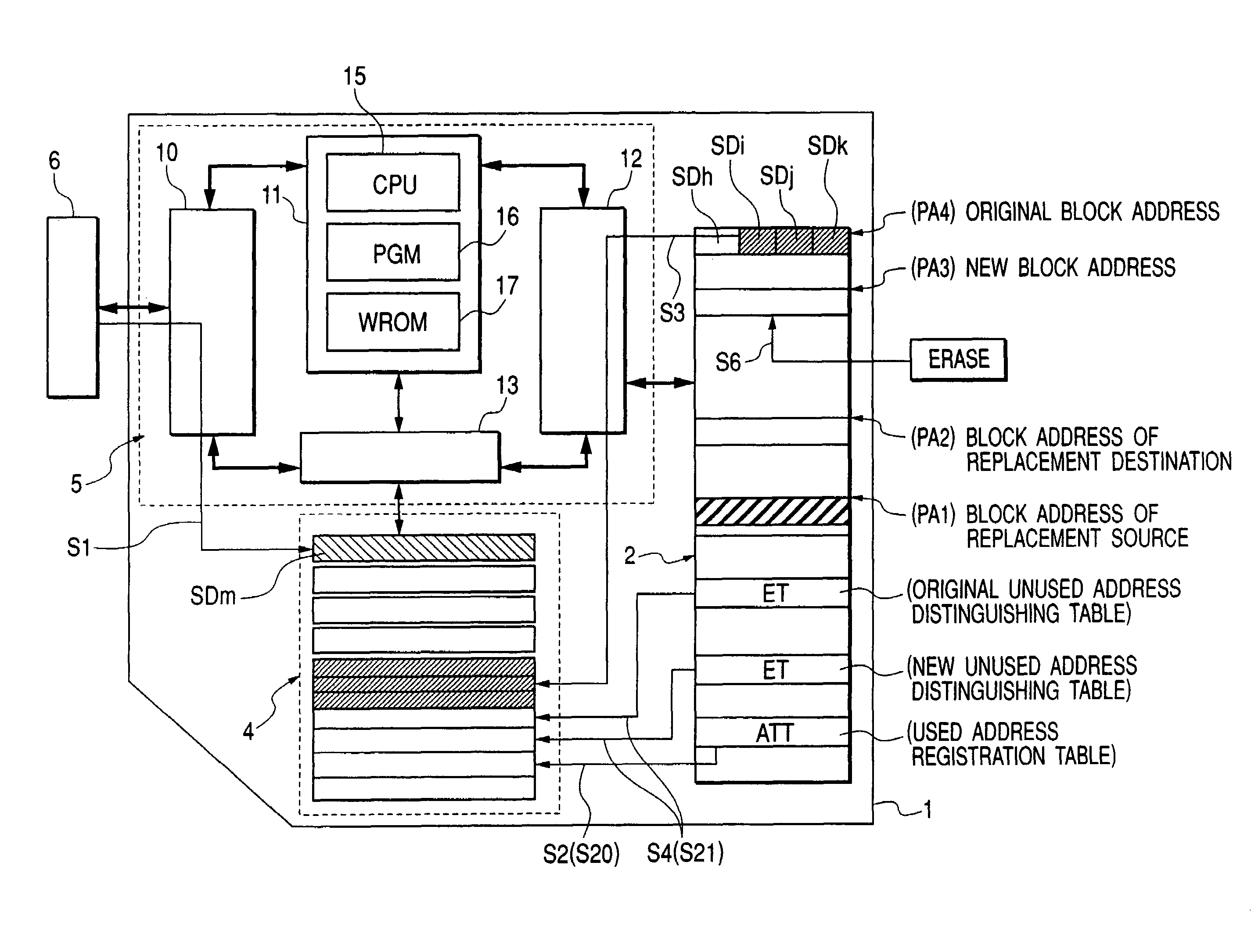
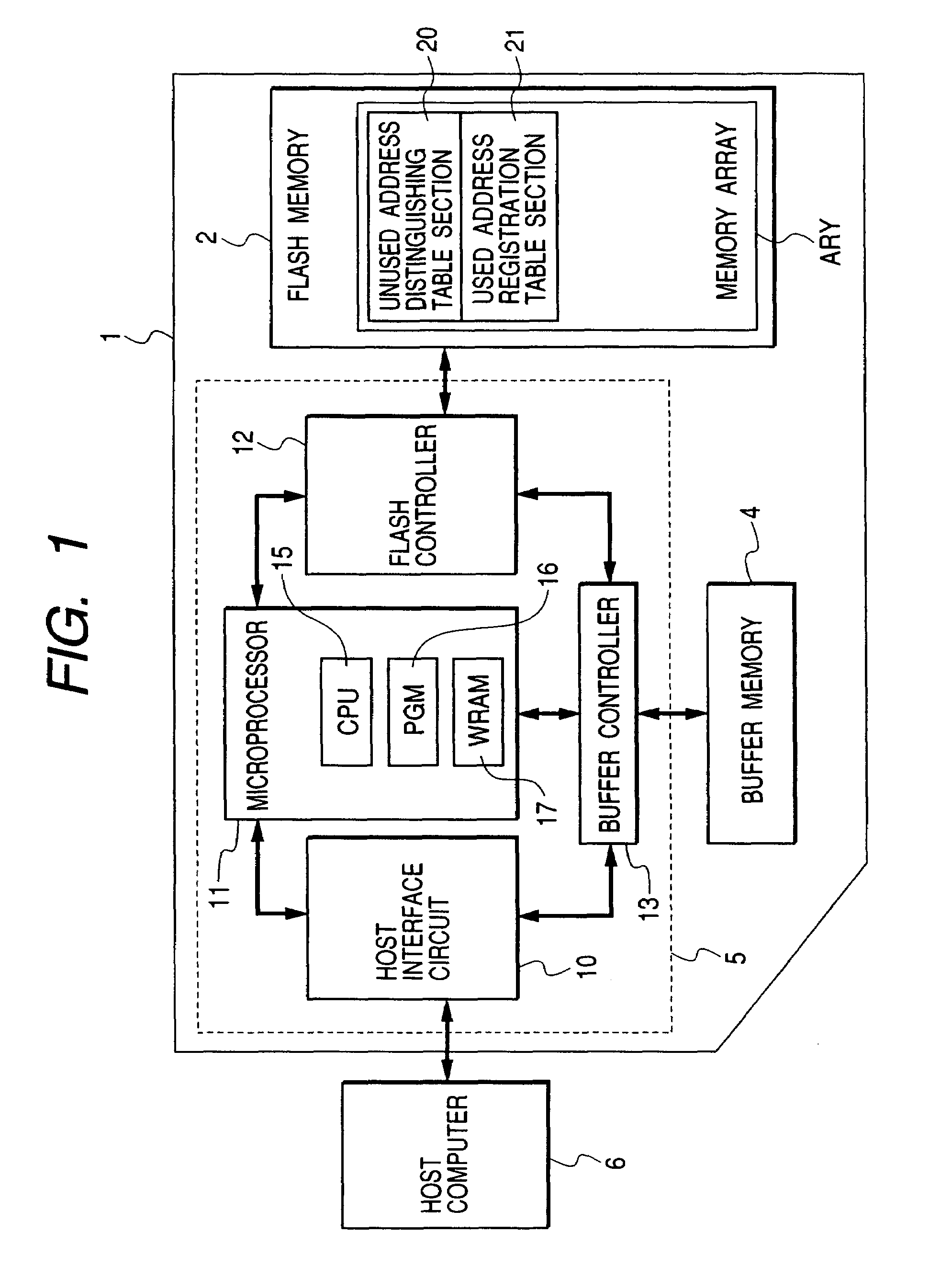
[0040]FIG. 1 shows a flash memory card, which is an example of memory device pertaining to the present invention. The flash memory card 1 is configured of an erasable and writable nonvolatile memory, e.g. a flash memory 2, a buffer memory 4 consisting of a dynamic random access memory (DRAM) or a static random access memory (SRAM), and a card controller (control circuit) 5 to perform memory control and external interface control, all being mounted on a package substrate.

[0041]The buffer memory 4 and the flash memory 2 are under access control by the card controller 5. The flash memory 2, though not specifically illustrated, has a memory array ARY in which a large number of electrically erasable and writable nonvolatile memory cell transistors are arranged in a matrix. Each of the memory cell transistors (sometimes alternatively referred to as flash memory cells), though not specifically illustrated, is configured of a source and a drain formed over a semiconductor substrate or in a ...


PUM

PropertyMeasurementUnit
rewrite frequencyaaaaaaaaaa
rewrite frequenciesaaaaaaaaaa
frequencyaaaaaaaaaa

Abstract

A risk of data garbling due to cumulative impact of disturbances occurring in memory areas in which no rewrite occurs is to be prevented. A memory device has an erasable and writable nonvolatile memory and a control circuit, wherein the control circuit is enabled to perform processing at a prescribed timing to replace memory areas. The replacement processing is accomplished by writing stored data in a first memory area in which rewriting is relatively infrequent into an unused second memory area, and making the second memory area into which the writing has been done a used area in place of the first memory area. Since this replacement processing is intended to replace memory areas in which rewriting is infrequent with other memory areas as described above, it is possible to prevent the risk of data garbling due to the cumulative impact of disturbances occurring in memory areas in which no rewrite occurs.

Description

CROSS-REFERENCE TO RELATED APPLICATION[0001]This application is a continuation of application Ser. No. 10 / 809,416 filed Mar. 26, 2004 now abandoned.BACKGROUND OF THE INVENTION[0002]The present invention relates to a nonvolatile memory device and to a technique that can be effectively applied to, for instance, flash memory cards, hard disk-compatible flash disks, and the like.[0003]Rewriting of stored information in an electrically rewritable nonvolatile memory, typically a flash memory, involves electrical stresses in memory cells, whose performance characteristics would deteriorate with an increase in the frequency of rewriting. If rewrites locally concentrate, only some data blocks markedly deteriorate in characteristics. There is a technique to solve this problem by which data and addresses are automatically relocated into other areas when the frequency of rewriting has reached a certain level, and the useful life of the nonvolatile memory is extended in terms of the permissible ...

Claims


Application Information

Patent Timeline
Patent Type & Authority Patents(United States)
IPC IPC(8): G06F12/02G06F12/16G06F12/00G06K19/07G11C16/02G11C16/10G11C16/34
CPCG06F12/0246G11C16/349G11C16/3495G06F2212/1036G06F2212/7211B65C9/1865B65C9/40B65H18/10B65H2301/41461B65H2701/192
Inventor SHINAGAWA, CHIAKISHIRAISHI, ATSUSHIKANAMORI, MOTOKI
Owner RENESAS ELECTRONICS CORP
Why Eureka
Try Eureka