Light emissive signage devices based on lightwave coupling
a technology of lightwave coupling and signage device, which is applied in waveguides, identification means, instruments, etc., to achieve the effect of low brightness, supply legibility, and low concomitant loss of emitted luminan
- Summary
- Abstract
- Description
- Claims
- Application Information
AI Technical Summary
Benefits of technology
Problems solved by technology
Method used
Image
Examples
example 1
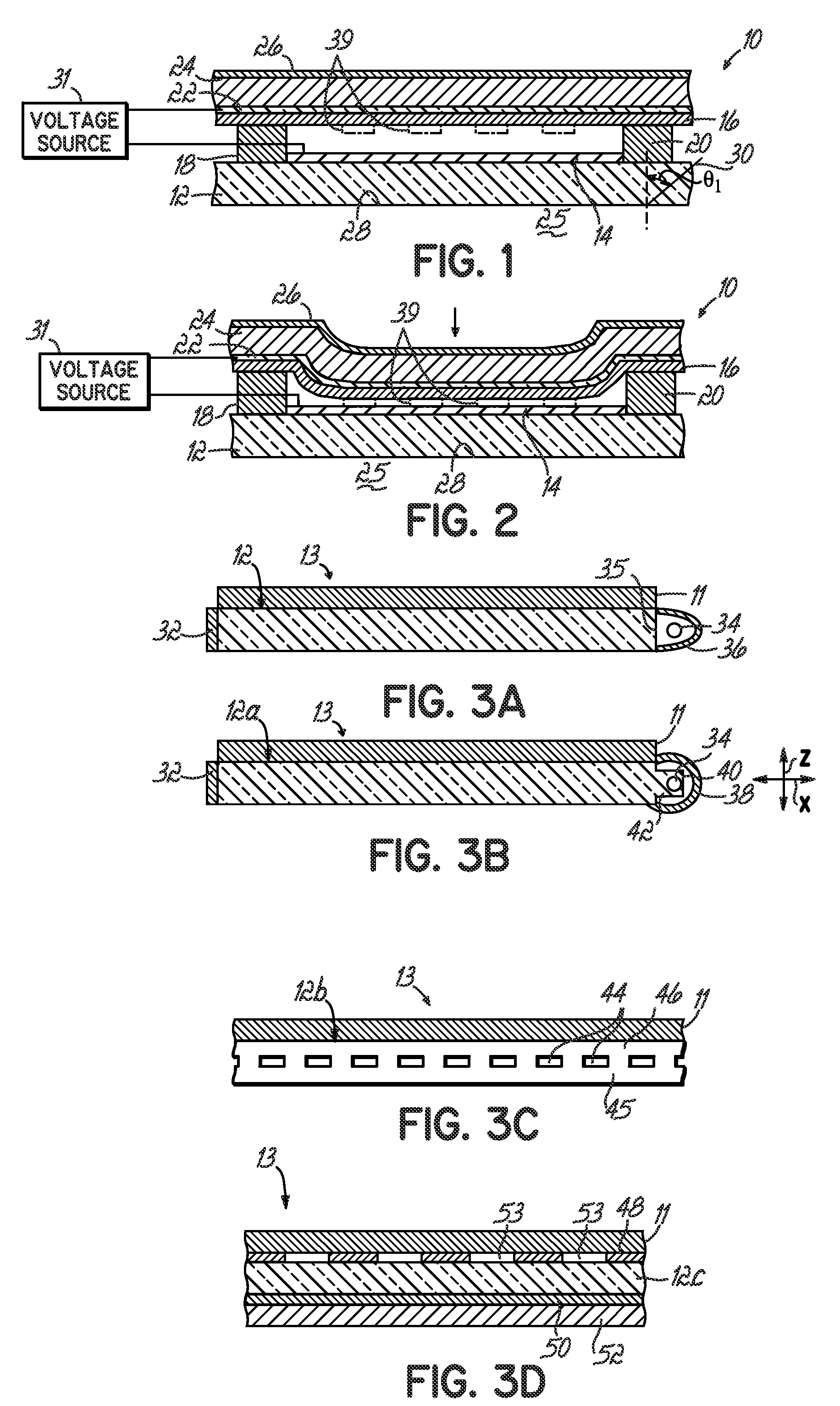
[0152]A polymer binder (Ferro 75001 polyvinylbutyrolterpolymer PVB, binder) was mixed with about 1 percent to about 10 percent by volume solution of acetone and the maximum soluble concentration of BASF Lumogen 300 and BASF Lumogen 083 fluoropolymers to form a photoluminescent resin. The photoluminescent resin was doctor blade applied to a glass substrate and baked at 150° C. for 10 minutes to volatilize all solvents in order to form a solid gel layer. The photoluminescent layer was then bonded to DuPont KAPTON® tape film and pulled from the glass substrate it was formed on to create a usable film flexible film. The resulting photoluminescent film was placed on an acrylic waveguide propagating blue / violet light from a cold-cathode-fluorescent-lamp.
[0153]In regions where pressure was applied onto the photoluminescent layer onto the substrate, the photoluminescent layer brightly fluoresced. The photoluminescent layer was further pressed against the glass in several regions, optically ...
example 2
[0154]BASF Lumogen dyes were dissolved at maximum solubility in Acetone. BASF dye Lumogen 570 was used for blue emission, Lumogen 083 for green emission, and Lumogen 300 for red emission. This mixture was then added to and dissolved in acrylic beads in an airtight container. Once the mixture was completely dissolved, a non-volatile thinner of DuPont 8250 was added, mixed, and the acetone allowed to volatize over a period of 12 hours. This photoluminescent resin was then screen-printed onto an acrylic waveguide and baked at 120° C. for 15 minutes to remove the DuPont 8250, forming a hard and transparent photoluminescent layer. The waveguide was then mirrored using an A1 adhesive tape and InGaN LEDs attached through apertures in the tape.
[0155]This signage form of an LWC display exhibited the following performance:[0156]Waveguide Dimensions: about 2″×4″, about 2 mm thickness[0157]Pump Specifications: 10 InGaN violet LEDs, 20 mA each[0158]Power requirement: 3.5 V, 200 mA, 0.7 W[0159]Lu...
example 3
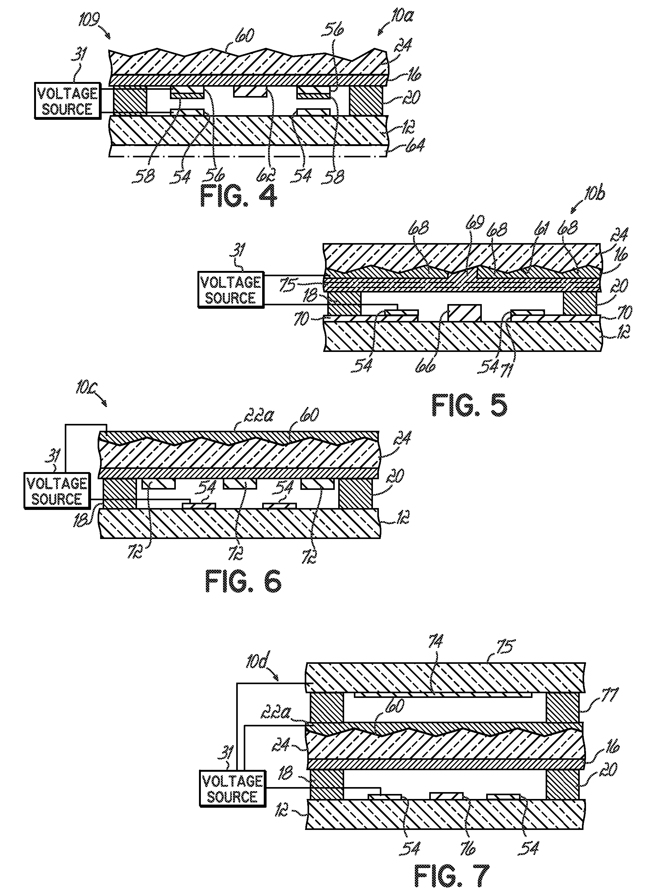
[0164]The photoluminescent resins of Example 2 were screen-printed onto a first acrylic waveguide and baked at 120° C. for 15 minutes to form a hard photoluminescent layer. A second waveguide was then mirrored using an A1 adhesive tape and InGaN LEDs attached through apertures in the tape. An silicone oil drop was placed at several regions between the first waveguide and second waveguide, the waveguides then sandwiched together, in order to measure the effective device contrast ratio achievable using electro-static or electrowetting based modulation in an LWC device.[0165]Waveguide Dimensions: about 2″×4″, about 2 mm thickness[0166]Pump Specifications: 4 InGaN violet LEDs, 10 mA each[0167]Power requirement: 3.5 V, 40 mA, 0.14 W
[0168]
Non CoupledCoupledContrast Ratiored 0.1 cd / m2 50 cd / m2500:1green 0.3 cd / m2105 cd / m2300:1blue0.15 cd / m2 35 cd / m2200:1[0169]Waveguide Luminance: violet 0.1 cd / m2 (at imperfections)[0170]Appearance: Transparent
[0171]An interesting comparison may be made to ...
PUM
 Abstract
Description
Claims
Application Information
 - R&D
- Intellectual Property
- Life Sciences
- Materials
- Tech Scout
- Unparalleled Data Quality
- Higher Quality Content
- 60% Fewer Hallucinations
Browse by: Latest US Patents, China's latest patents, Technical Efficacy Thesaurus, Application Domain, Technology Topic, Popular Technical Reports.
© 2025 PatSnap. All rights reserved.Legal|Privacy policy|Modern Slavery Act Transparency Statement|Sitemap|About US| Contact US: help@patsnap.com


