Optical semiconductor device with improved illumination efficiency
a technology of optical semiconductors and illumination efficiency, applied in the direction of semiconductor devices, basic electric elements, electrical appliances, etc., can solve the problems of difficult to obtain a 100% optical reflectivity, follow-up problems, and light may be attenuated due to, etc., to achieve the effect of suitable luminance of light emission
- Summary
- Abstract
- Description
- Claims
- Application Information
AI Technical Summary
Benefits of technology
Problems solved by technology
Method used
Image
Examples
first embodiment
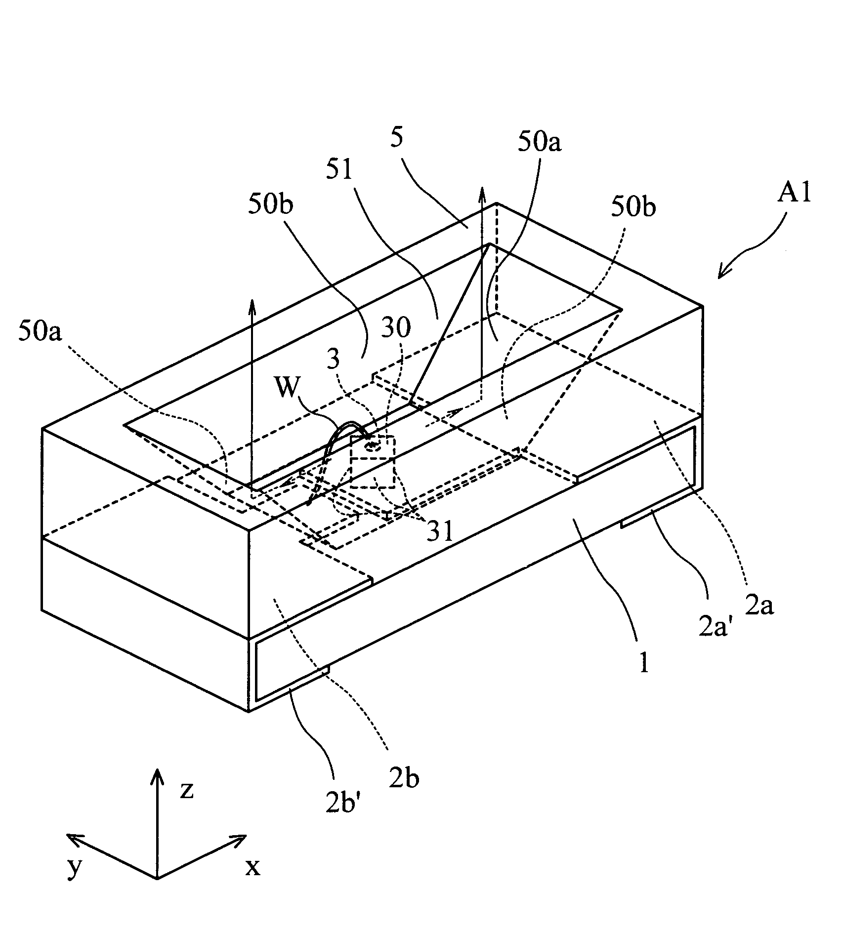
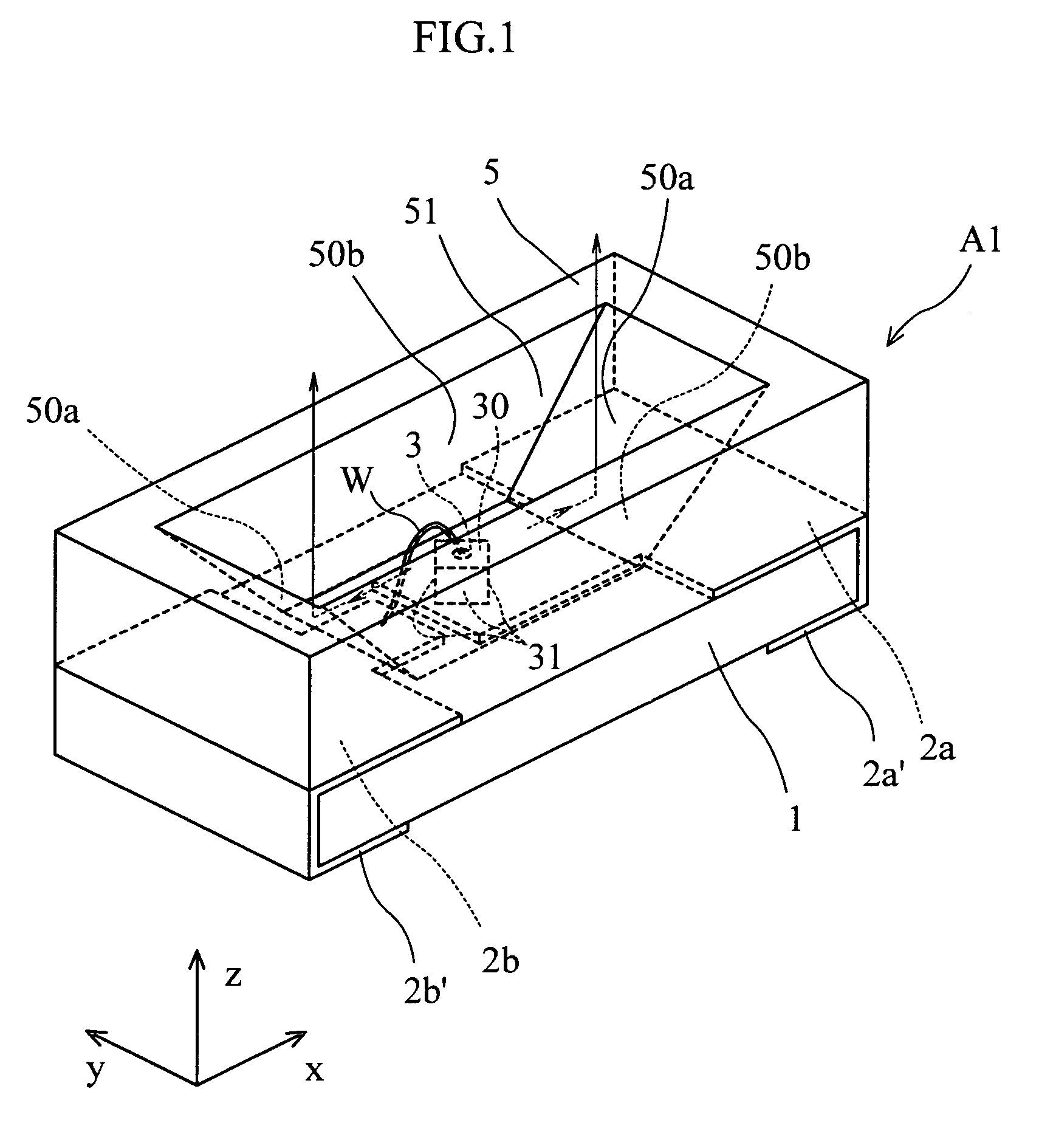
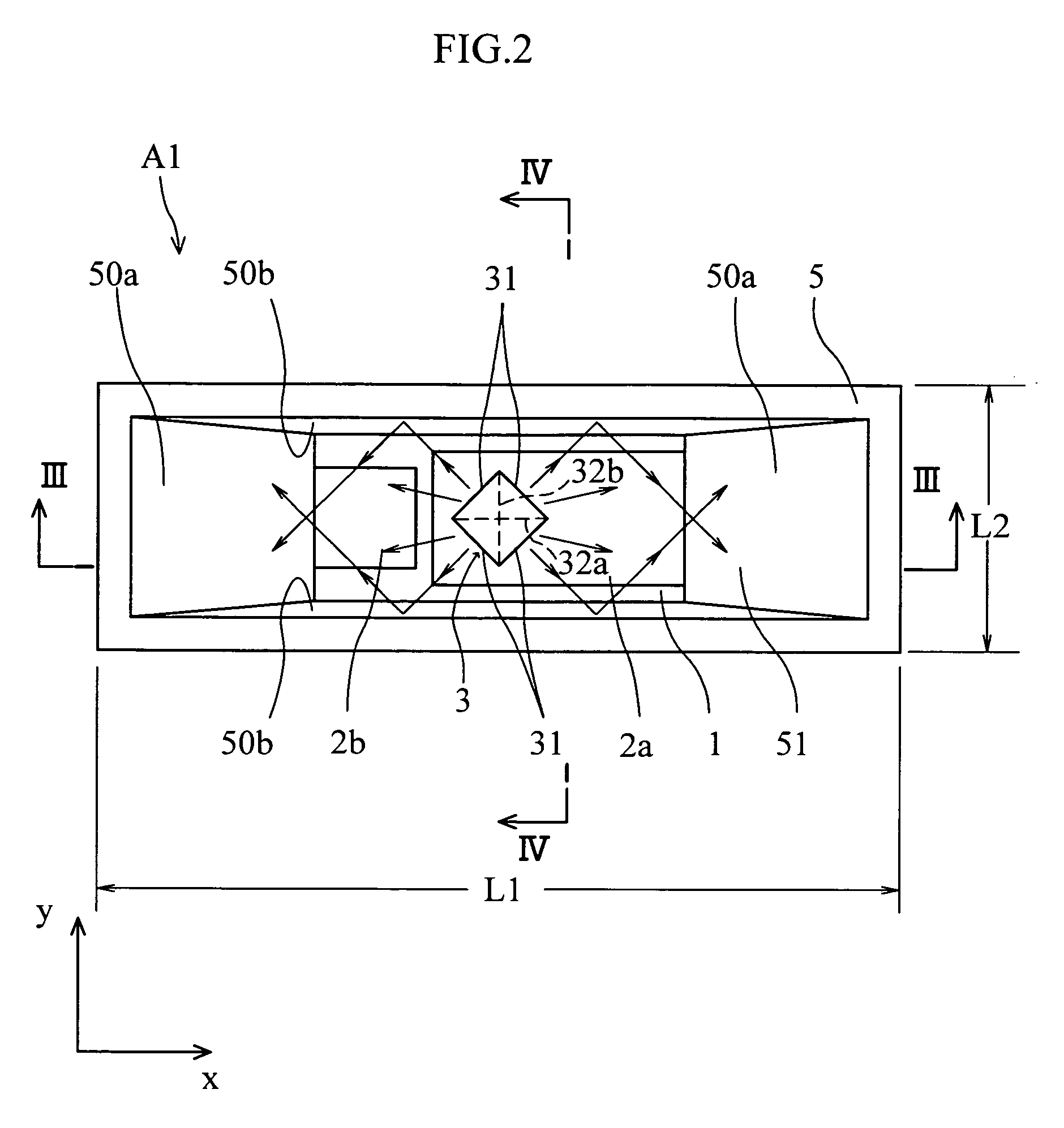
[0033]FIGS. 1-4 illustrate an optical semiconductor device A1 according to the present invention. In FIG. 1, a coordinate system is set along the directions x, y, and z, relative to the optical semiconductor device A1. Each of the three directions is perpendicular to the other two directions, and the direction z is the vertical direction of the device (the arrangement is the same for other embodiments). FIG. 2 shows the optical semiconductor device A1 viewed in the direction z (or viewed parallel to the direction z) from a viewpoint above the optical semiconductor device A1. FIG. 3 is a sectional view taken along lines III-III in FIG. 2, and FIG. 4 is a sectional view taken along lines IV-IV in FIG. 2.
[0034]The optical semiconductor device A1 includes a rectangular insulating base plate 1, an LED chip 3, a reflector 5, and a light-permeable member 6. The light-permeable member 6 is not shown in FIGS. 1 and 2.
[0035]The base plate 1 is made of a glass epoxy resin, for example. The bas...
second embodiment
[0046]FIG. 5 illustrates an optical semiconductor device A2 according to the present invention. The optical semiconductor device A2 includes three LED chips 3 accommodated in the reflector 5. These LED chips 3 are aligned and spaced from each other in the direction x, and every one of them is arranged the same as the LED chip shown in FIG. 2 (specifically, the side surfaces 31 are inclined at 45° relative to the x axis and the y axis).
[0047]This structure can also make the light, that is emitted from the side surfaces 31 of the LED chips 3 and travels toward the second reflecting surface 50b, to be guided to the first reflecting surface 50a, and to be upwardly reflected at the first reflecting surfaced 50a to above the optical semiconductor device A2. The LED chips 3 may emit light of a same color, or of different colors (R, G, B). The LED chips 3 may also drive at the same time, or only one or two selected chips may drive at a time.
third embodiment
[0048]FIG. 6A illustrates an optical semiconductor device A3 of the present invention. In the optical semiconductor device A3, each of the side surfaces 31 of the LED chip 3 is arranged parallel to any one of the directions x and y (and parallel to the direction z). Each of the second reflecting surfaces 50b of the reflector 5 is formed with a projection 53 protruding toward the LED chip 3. The projection 53 faces one side surface (one of the two side surfaces 31a spaced from each other in the direction y) of the LED chip 3. The projection 53 is triangular in section and includes a pair of walls (reflecting surfaces) 53a for light reflection. Each of the reflecting surfaces 53a is parallel to the direction z, while non-parallel to both of the directions x and y. The reflecting surfaces 53a are inclined relative to the direction x at 45°, for example. Thus, the reflecting surfaces 53a are non-parallel to the side surfaces 31a that are parallel to the directions x and y.
[0049]Due to ...
PUM
 Abstract
Description
Claims
Application Information
 - R&D
- Intellectual Property
- Life Sciences
- Materials
- Tech Scout
- Unparalleled Data Quality
- Higher Quality Content
- 60% Fewer Hallucinations
Browse by: Latest US Patents, China's latest patents, Technical Efficacy Thesaurus, Application Domain, Technology Topic, Popular Technical Reports.
© 2025 PatSnap. All rights reserved.Legal|Privacy policy|Modern Slavery Act Transparency Statement|Sitemap|About US| Contact US: help@patsnap.com


